


DS610-3 (v2.0) July 16, 2007 www.xilinx.com 11
Product Specification
© 2007 Xilinx, Inc. All rights reserved. All Xilinx trademarks, registered trademarks, patents, and disclaimers are as listed at http://www.xilinx.com/legal.htm.
All other trademarks are the property of their respective owners. All specifications are subject to change without notice.
DC Electrical Characteristics
In this section, specifications may be designated as
Advance, Preliminary, or Production. These terms are
defined as follows:
Advance: Initial estimates are based on simulation, early
characterization, and/or extrapolation from the
characteristics of other families. Values are subject to
change. Use as estimates, not for production.
Preliminary: Based on characterization. Further changes
are not expected.
Production: These specifications are approved once the
silicon has been characterized over numerous production
lots. Parameter values are considered stable with no future
changes expected.
All parameter limits are representative of worst-case supply
voltage and junction temperature conditions. Unless
otherwise noted, the published parameter values apply
to all Spartan™-3A DSP devices. AC and DC
characteristics are specified using the same numbers
for both commercial and industrial grades.
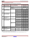
Absolute Maximum Ratings
Stresses beyond those listed under Tabl e 3: Absolute
Maximum Ratings may cause permanent damage to the
device. These are stress ratings only; functional operation
of the device at these or any other conditions beyond those
listed under the Recommended Operating Conditions is not
implied. Exposure to absolute maximum conditions for
extended periods of time adversely affects device reliability.
<BL
Blue
>
Spartan-3A DSP FPGA Family:
DC and Switching Characteristics
DS610-3 (v2.0) July 16, 2007
0
Product Specification
R
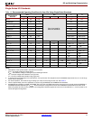
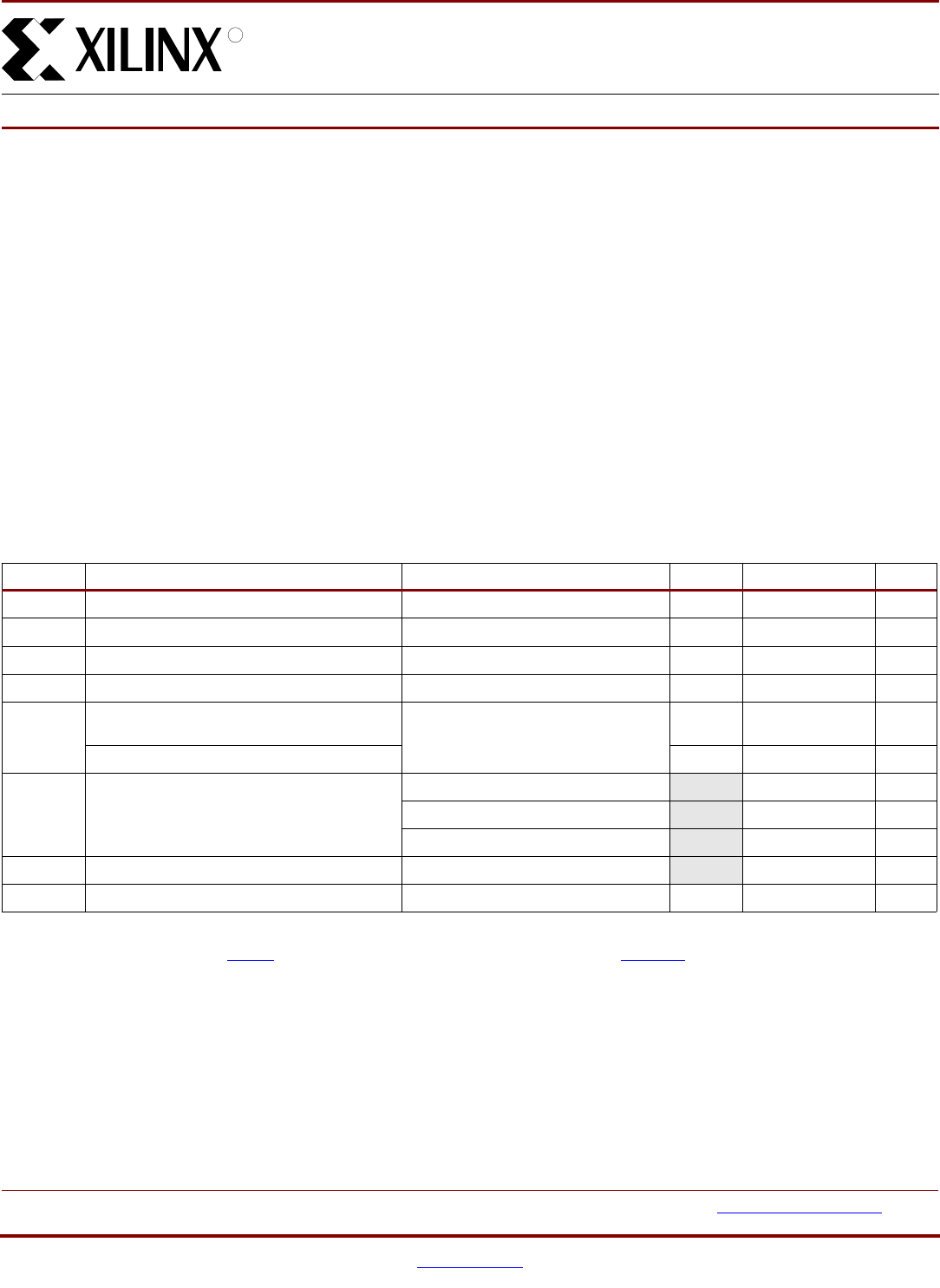
Table 3:
Absolute Maximum Ratings
Symbol Description Conditions Min Max Units
V
CCINT
Internal supply voltage –0.5 1.32 V
V
CCAUX
Auxiliary supply voltage –0.5 3.75 V
V
CCO
Output driver supply voltage –0.5 3.75 V
V
REF
Input reference voltage –0.5 V
CCO
+ 0.5 V
V
IN
Voltage applied to all User I/O pins and
Dual-Purpose pins
Driver in a high-impedance state
–0.95 4.6 V
Voltage applied to all Dedicated pins –0.5 4.6 V
V
ESD
Electrostatic Discharge Voltage Human body model – ±2000 V
Charged device model
– ±500 V
Machine model
– ±200 V
T
J
Junction temperature –125°C
T
STG
Storage temperature –65 150 °C
Notes:
1. For soldering guidelines, see UG112:
Device Packaging and Thermal Characteristics
and XAPP427:
Implementation and Solder Reflow
Guidelines for Pb-Free Packages
.