


Introduction and Ordering Information
4 www.xilinx.com DS610-1 (v2.0) July 16, 2007
Product Specification
R
Architectural Overview
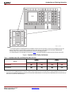
The Spartan-3A DSP family architecture consists of five
fundamental programmable functional elements:
• XtremeDSP DSP48A Slice provides an 18-bit x 18-bit
multiplier, 18-bit pre-adder, 48-bit
post-adder/accumulator, and cascade capabilities for
various DSP applications.
• Block RAM provides data storage in the form of
18-Kbit dual-port blocks.
• Configurable Logic Blocks (CLBs) contain flexible
Look-Up Tables (LUTs) that implement logic plus
storage elements used as flip-flops or latches. CLBs
perform a wide variety of logical functions as well as
store data.
• Input/Output Blocks (IOBs) control the flow of data
between the I/O pins and the internal logic of the
device. IOBs support bidirectional data flow plus
3-state operation. Supports a variety of signal
standards, including several high-performance
differential standards. Double Data-Rate (DDR)
registers are included.
• Digital Clock Manager (DCM) Blocks provide
self-calibrating, fully digital solutions for distributing,
delaying, multiplying, dividing, and phase-shifting clock
signals.
These elements are organized as shown in Figure 1. A dual
ring of staggered IOBs surrounds a regular array of CLBs.
The XC3SD1800A has four columns of DSP48As, and the
XC3SD3400A has five columns of DSP48As. Each
DSP48A has an associated block RAM. The DCMs are
positioned in the center with two at the top and two at the
bottom of the device and in the two outer columns of the 4 or
5 columns of block RAM and DSP48As.
The Spartan-3A DSP family features a rich network of
routing that interconnect all five functional elements,
transmitting signals among them. Each functional element
has an associated switch matrix that permits multiple
connections to the routing.
Configuration
Spartan-3A DSP FPGAs are programmed by loading
configuration data into robust, reprogrammable, static
CMOS configuration latches (CCLs) that collectively control
all functional elements and routing resources. The FPGA’s
configuration data is stored externally in a PROM or some
other non-volatile medium, either on or off the board.
After applying power, the configuration data is written to the
FPGA using any of seven different modes:
• Master Serial from a Xilinx Platform Flash PROM
• Serial Peripheral Interface (SPI) from an
industry-standard SPI serial Flash
• Byte Peripheral Interface (BPI) Up from an
industry-standard x8 or x8/x16 parallel NOR Flash
• Slave Serial, typically downloaded from a processor
• Slave Parallel, typically downloaded from a processor
• Boundary Scan (JTAG), typically downloaded from a
processor or system tester
Furthermore, Spartan-3A DSP FPGAs support MultiBoot
configuration, allowing two or more FPGA configuration
bitstreams to be stored in a single SPI serial Flash or a
parallel NOR Flash. The FPGA application controls which
configuration to load next and when to load it.
Additionally, each Spartan-3A DSP FPGA contains a
unique, factory-programmed Device DNA identifier useful
for tracking purposes, anti-cloning designs, or IP protection.
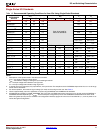
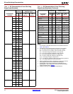
I/O Capabilities
The Spartan-3A DSP FPGA SelectIO interface supports
many popular single-ended and differential standards.
Table 2 shows the number of user I/Os as well as the
number of differential I/O pairs available for each
device/package combination. Some of the user I/Os are
unidirectional input-only pins as indicated in Table 2.
Spartan-3A DSP FPGAs support the following single-ended
standards:
• 3.3V low-voltage TTL (LVTTL)
• Low-voltage CMOS (LVCMOS) at 3.3V, 2.5V, 1.8V,
1.5V, or 1.2V
• 3.3V PCI at 33 MHz or 66 MHz
• HSTL I, II, and III at 1.5V and 1.8V, commonly used in
memory applications
• SSTL I and II at 1.8V, 2.5V, and 3.3V, commonly used
for memory applications
Spartan-3A DSP FPGAs support the following differential
standards:
• LVDS, mini-LVDS, RSDS, and PPDS I/O at 2.5V or
3.3V
• Bus LVDS I/O at 2.5V
• TMDS I/O at 3.3V
• Differential HSTL and SSTL I/O
• LVPECL inputs at 2.5V or 3.3V