


DC and Switching Characteristics
DS610-3 (v2.0) July 16, 2007 www.xilinx.com 23
Product Specification
R
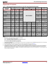
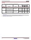
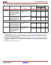
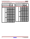
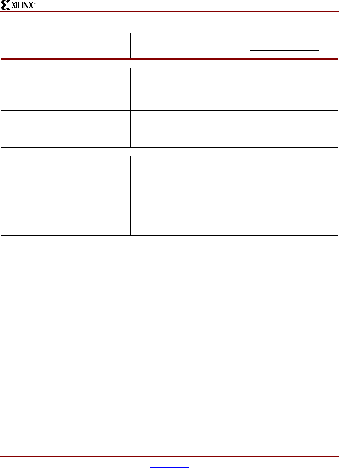
Table 18:
Pin-to-Pin Setup and Hold Times for the IOB Input Path (System Synchronous)
Symbol Description Conditions Device
Speed Grade
Units
-5 -4
Min Min
Setup Times
T
PSDCM
When writing to the Input
Flip-Flop (IFF), the time from
the setup of data at the Input
pin to the active transition at a
Global Clock pin. The DCM is in
use. No Input Delay is
programmed.
LVCMOS25
(2)
,
IFD_DELAY_VALUE = 0,
with DCM
(4)
XC3SD1800A 2.65 3.11 ns
XC3SD3400A 2.25 2.49 ns
T
PSFD
When writing to IFF, the time
from the setup of data at the
Input pin to an active transition
at the Global Clock pin. The
DCM is not in use. The Input
Delay is programmed.
LVCMOS25
(2)
,
IFD_DELAY_VALUE = 6,
without DCM
XC3SD1800A 2.98 3.39 ns
XC3SD3400A 2.78 3.08 ns
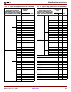
Hold Times
T
PHDCM
When writing to IFF, the time
from the active transition at the
Global Clock pin to the point
when data must be held at the
Input pin. The DCM is in use.
No Input Delay is programmed.
LVCMOS25
(3)
,
IFD_DELAY_VALUE = 0,
with DCM
(4)
XC3SD1800A -0.38 -0.38 ns
XC3SD3400A -0.26 -0.26 ns
T
PHFD
When writing to IFF, the time
from the active transition at the
Global Clock pin to the point
when data must be held at the
Input pin. The DCM is not in
use. The Input Delay is
programmed.
LVCMOS25
(3)
,
IFD_DELAY_VALUE = 6,
without DCM
XC3SD1800A -0.71 -0.71 ns
XC3SD3400A -0.65 -0.65 ns
Notes:
1. The numbers in this table are tested using the methodology presented in Table 25 and are based on the operating conditions set forth in
Table 7 and Table 10.
2. This setup time requires adjustment whenever a signal standard other than LVCMOS25 is assigned to the Global Clock Input or the data
Input. If this is true of the Global Clock Input, subtract the appropriate adjustment from Table 21. If this is true of the data Input, add the
appropriate Input adjustment from the same table.
3. This hold time requires adjustment whenever a signal standard other than LVCMOS25 is assigned to the Global Clock Input or the data
Input. If this is true of the Global Clock Input, add the appropriate Input adjustment from Table 21. If this is true of the data Input, subtract
the appropriate Input adjustment from the same table. When the hold time is negative, it is possible to change the data before the clock’s
active edge.
4. DCM output jitter is included in all measurements.