


DC and Switching Characteristics
22 www.xilinx.com DS610-3 (v2.0) July 16, 2007
Product Specification
R
I/O Timing
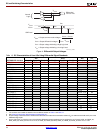
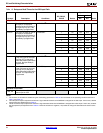
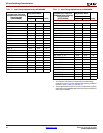
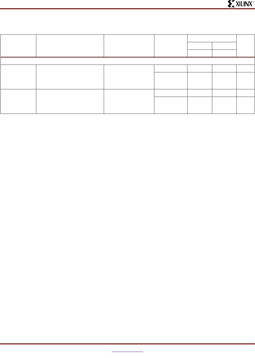
Table 17:
Pin-to-Pin Clock-to-Output Times for the IOB Output Path
Symbol Description Conditions Device
Speed Grade
Units
-5 -4
Max Max
Clock-to-Output Times
T
ICKOFDCM
When reading from the Output
Flip-Flop (OFF), the time from the
active transition on the Global
Clock pin to data appearing at the
Output pin. The DCM is in use.
LVCMOS25
(2)
, 12mA
output drive, Fast slew
rate, with DCM
(3)
XC3SD1800A 3.28 3.51 ns
XC3SD3400A 3.36 3.82 ns
T
ICKOF
When reading from OFF, the time
from the active transition on the
Global Clock pin to data appearing
at the Output pin. The DCM is not
in use.
LVCMOS25
(2)
, 12mA
output drive, Fast slew
rate, without DCM
XC3SD1800A 5.23 5.58 ns
XC3SD3400A 5.51 6.13 ns
Notes:
1. The numbers in this table are tested using the methodology presented in Table 25 and are based on the operating conditions set forth in
Table 7 and Table 10.
2. This clock-to-output time requires adjustment whenever a signal standard other than LVCMOS25 is assigned to the Global Clock Input or a
standard other than LVCMOS25 with 12 mA drive and Fast slew rate is assigned to the data Output. If the former is true,
add
the appropriate
Input adjustment from Table 21. If the latter is true,
add
the appropriate Output adjustment from Table 24.
3. DCM output jitter is included in all measurements.