


DC and Switching Characteristics
DS610-3 (v2.0) July 16, 2007 www.xilinx.com 13
Product Specification
R
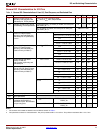
General DC Characteristics for I/O Pins
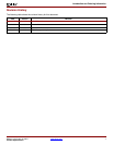
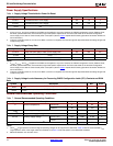
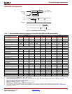
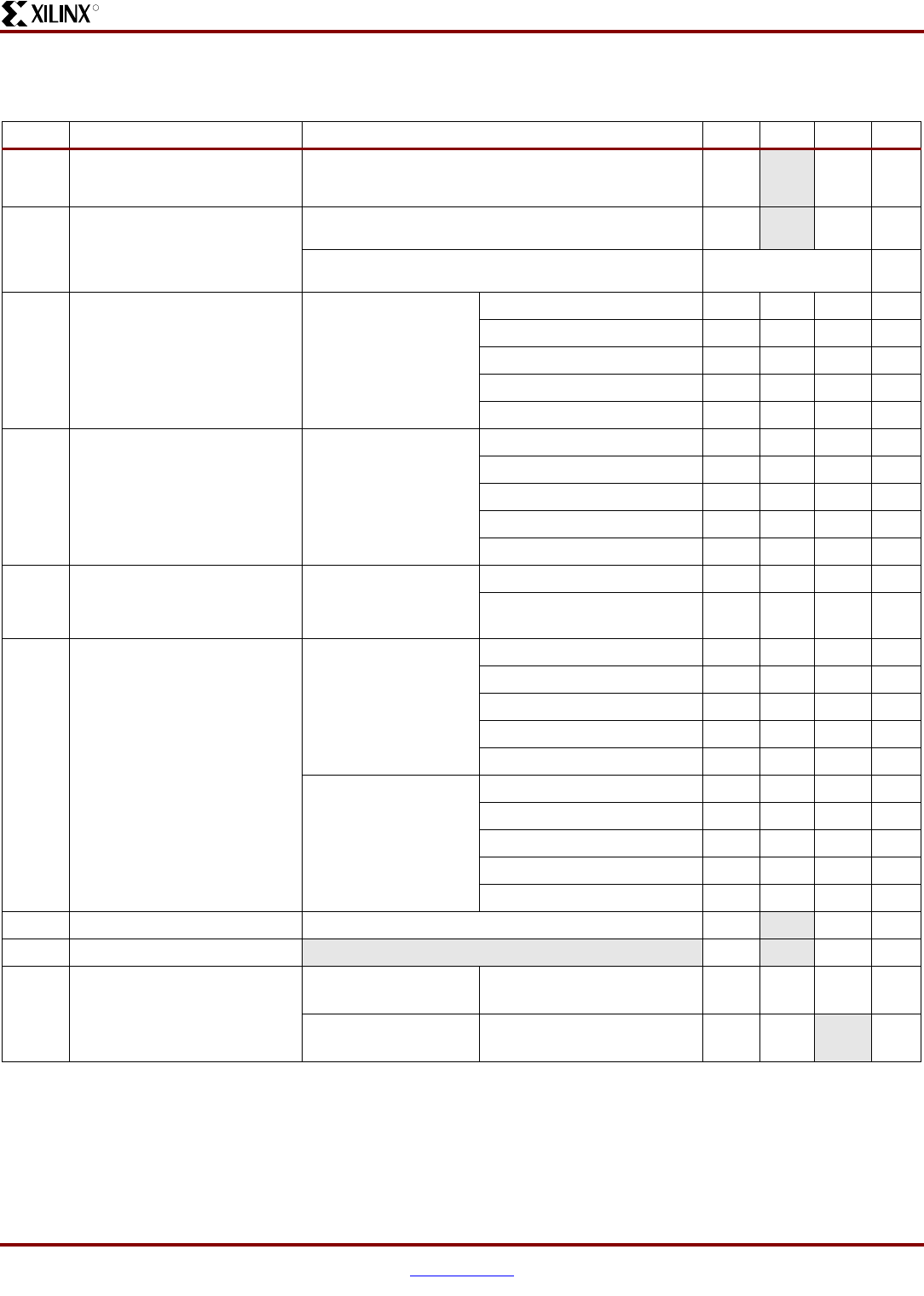
Table 8:
General DC Characteristics of User I/O, Dual-Purpose, and Dedicated Pins
Symbol Description Test Conditions Min Typ Max Units
I
L
Leakage current at User I/O,
Input-only, Dual-Purpose, and
Dedicated pins, FPGA powered
Driver is in a high-impedance state,
V
IN
= 0V or V
CCO
max, sample-tested
–10 -+10μA
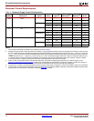
I
HS
Leakage current on pins during
hot socketing, FPGA unpowered
All pins except INIT_B, PROG_B, DONE, and JTAG pins
when PUDC_B = 1.
–10
-+10μA
INIT_B, PROG_B, DONE, and JTAG pins or other pins
when PUDC_B = 0.
Add I
HS
+ I
RPU
μA
I
RPU
(2)
Current through pull-up resistor
at User I/O, Dual-Purpose,
Input-only, and Dedicated pins.
Dedicated pins are powered by
V
CCAUX
.
V
IN
= GND V
CCO
or V
CCAUX
= 3.0V to 3.6V –151 –315 –710 μA
V
CCO
or V
CCAUX
= 2.3V to 2.7V –82 –182 –437 μA
V
CCO
= 1.7V to 1.9V –36 –88 –226 μA
V
CCO
= 1.4V to 1.6V –22 –56 –148 μA
V
CCO
= 1.14V to 1.26V –11 –31 –83 μA
R
PU
(2)
Equivalent pull-up resistor value
at User I/O, Dual-Purpose,
Input-only, and Dedicated pins
(based on I
RPU
per Note 2)
V
IN
= GND V
CCO
= 3.0V to 3.6V 5.1 11.4 23.9 kΩ
V
CCO
= 2.3V to 2.7V 6.2 14.8 33.1 kΩ
V
CCO
= 1.7V to 1.9V 8.4 21.6 52.6 kΩ
V
CCO
= 1.4V to 1.6V 10.8 28.4 74.0 kΩ
V
CCO
= 1.14V to 1.26V 15.3 41.1 119.4 kΩ
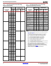
I
RPD
(2)
Current through pull-down
resistor at User I/O,
Dual-Purpose, Input-only, and
Dedicated pins
V
IN
= V
CCO
V
CCAUX
= 3.0V to 3.6V 167 346 659 μA
V
CCAUX
= 2.25V to 2.75V
100 225 457 μA
R
PD
(2)
Equivalent pull-down resistor
value at User I/O, Dual-Purpose,
Input-only, and Dedicated pins
(based on I
RPD
per Note 2)
V
CCAUX
= 3.0V to 3.6V V
IN
= 3.0V to 3.6V 5.5 10.4 20.8 kΩ
V
IN
= 2.3V to 2.7V 4.1 7.8 15.7 kΩ
V
IN
= 1.7V to 1.9V 3.0 5.7 11.1 kΩ
V
IN
= 1.4V to 1.6V 2.7 5.1 9.6 kΩ
V
IN
= 1.14V to 1.26V 2.4 4.5 8.1 kΩ
V
CCAUX
= 2.25V to 2.75V V
IN
= 3.0V to 3.6V 7.9 16.0 35.0 kΩ
V
IN
= 2.3V to 2.7V 5.9 12.0 26.3 kΩ
V
IN
= 1.7V to 1.9V 4.2 8.5 18.6 kΩ
V
IN
= 1.4V to 1.6V 3.6 7.2 15.7 kΩ
V
IN
= 1.14V to 1.26V 3.0 6.0 12.5 kΩ
I
REF
V
REF
current per pin All V
CCO
levels –10 -+10μA
C
IN
Input capacitance -3-10pF
R
DT
Resistance of optional differential
termination circuit within a
differential I/O pair. Not available
on Input-only pairs.
V
CCO
= 3.3V ± 10%
LVDS_33, MINI_LVDS_33,
RSDS_33
90 100 115 Ω
V
CCO
= 2.5V ± 10%
LVDS_25, MINI_LVDS_25,
RSDS_25
90 110 – Ω
Notes:
1. The numbers in this table are based on the conditions set forth in Table 7.
2. This parameter is based on characterization. The pull-up resistance R
PU
= V
CCO
/I
RPU
. The pull-down resistance R
PD
= V
IN
/ I
RPD
.