


DC and Switching Characteristics
DS610-3 (v2.0) July 16, 2007 www.xilinx.com 57
Product Specification
R
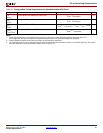
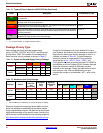
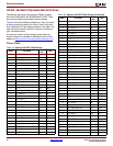
Revision History
The following table shows the revision history for this document.
Date Version Revision
04/02/07 1.0 Initial Xilinx release.
05/25/07 1.0.1 Minor edits.
06/18/07 1.2 Updated for v1.29 production speed files. Noted banking rules in Table 11 and Table 12. Added
DIFF_HSTL_I and DIFF_HSTL_III to Table 12, Table 13, and Table 25. Updated TMDS DC
characteristics in Table 13. Updated I/O Test Method values in Table 25. Added Simultaneously
Switching Output limits in Table 27. Updated DSP48A timing symbols, descriptions, and values in
Table 33. Added power-on timing in Table 44. Added CCLK specifications for Commercial in Table 45
through Table 47. Updated Slave Parallel timing in Table 50. Updated JTAG specifications in Table 55.
07/16/07 2.0 Added Low-power options and updated typical values for quiescent current in Table 9. Updated
DSP48A timing in Table 33 and Table 34.