


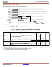
DC and Switching Characteristics
DS610-3 (v2.0) July 16, 2007 www.xilinx.com 47
Product Specification
R
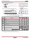
Configuration and JTAG Timing
General Configuration Power-On/Reconfigure Timing
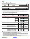
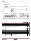
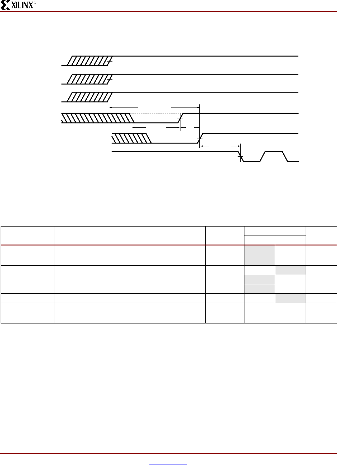
Figure 10:
Waveforms for Power-On and the Beginning of Configuration
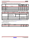
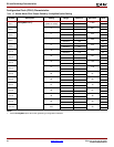
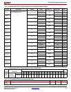
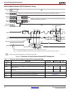
Table 44:
Power-On Timing and the Beginning of Configuration
Symbol Description Device
All Speed Grades
UnitsMin Max
T
POR
(2)
The time from the application of V
CCINT
, V
CCAUX
, and V
CCO
Bank 2 supply voltage ramps (whichever occurs last) to the
rising transition of the INIT_B pin
All -18ms
T
PROG
The width of the low-going pulse on the PROG_B pin All 0.5 - μs
T
PL
(2)
The time from the rising edge of the PROG_B pin to the
rising transition on the INIT_B pin
XC3SD1800A
-2ms
XC3SD3400A
-2ms
T
INIT
Minimum Low pulse width on INIT_B output All 300 -ns
T
ICCK
(3)
The time from the rising edge of the INIT_B pin to the
generation of the configuration clock signal at the CCLK
output pin
All 0.5 4 μs
Notes:
1. The numbers in this table are based on the operating conditions set forth in Table 7. This means power must be applied to all V
CCINT
, V
CCO
,
and V
CCAUX
lines.
2. Power-on reset and the clearing of configuration memory occurs during this period.
3. This specification applies only to the Master Serial, SPI, and BPI modes.
V
CCINT
(Supply)
(Supply)
(Supply)
V
CCAUX
V
CCO
Bank 2
PROG_B
(Output)
(Open-Drain)
(Input)
INIT_B
CCLK
DS529-3_01_112906
1.2V
2.5V
T
ICCK
T
PROG
T
PL
T
POR
1.0V
1.0V
2.0V
3.3V
or
Notes:
1. The V
CCINT
, V
CCAUX
, and V
CCO
supplies can be applied in any order.
2. The Low-going pulse on PROG_B is optional after power-on but necessary for reconfiguration without a power cycle.
3. The rising edge of INIT_B samples the voltage levels applied to the mode pins (M0 - M2).