Pinout Descriptions
60 www.xilinx.com DS610-4 (v2.0) July 16, 2007
Product Specification
R
Package Pins by Type
Each package has three separate voltage supply
inputs—VCCINT, VCCAUX, and VCCO—and a common
ground return, GND. The numbers of pins dedicated to
these functions vary by package, as shown in Table 57.
A majority of package pins are user-defined I/O or input
pins. However, the numbers and characteristics of these I/O
depend on the device type and the package in which it is
available, as shown in Table 58. The table shows the
maximum number of single-ended I/O pins available,
assuming that all I
/O-, INPUT-, DUAL-, VREF-, and
CLK-type pins are used as general-purpose I/O. AWAKE is
counted here as a Dual-Purpose I/O pin. Likewise, the table
shows the maximum number of differential pin-pairs
available on the package. Finally, the table shows how the
total maximum user-I/Os are distributed by pin type,
including the number of unconnected—N.C.—pins on the
device.
Electronic versions of the package pinout tables and foot-
prints are available for download from the Xilinx website.
Using a spreadsheet program, the data can be sorted and
reformatted according to any specific needs. Similarly, the
ASCII-text file is easily parsed by most scripting programs.
http://www.xilinx.com/bvdocs/publications/s3a
dsp_pin.zip
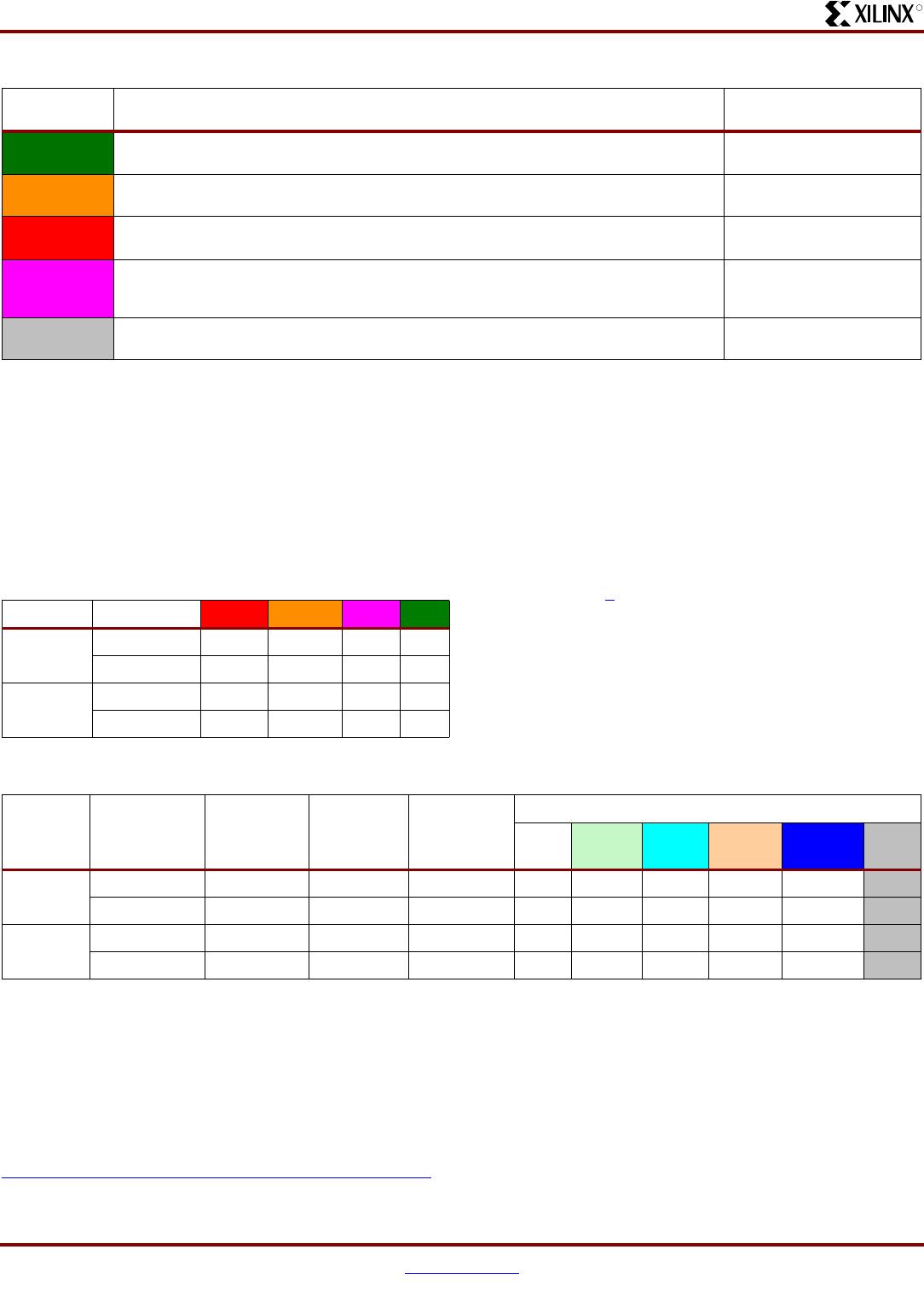
GND
Dedicated ground pin. The number of GND pins depends on the package used. All must
be connected.
GND
VCCAUX
Dedicated auxiliary power supply pin. The number of VCCAUX pins depends on the
package used. All must be connected.
VCCAUX
VCCINT
Dedicated internal core logic power supply pin. The number of VCCINT pins depends on
the package used. All must be connected to +1.2V.
VCCINT
VCCO
Along with all the other VCCO pins in the same bank, this pin supplies power to the output
buffers within the I/O bank and sets the input threshold voltage for some I/O standards. All
must be connected.
VCCO_#
N.C.
This package pin is not connected in this specific device/package combination but may be
connected in larger devices in the same package.
N.C.
Notes:
1. # = I/O bank number, an integer between 0 and 3.
Table 56:
Types of Pins on Spartan-3A DSP FPGAs
(Continued)
Type/Color
Code
Description Pin Name(s) in Type
Table 57:
Power and Ground Supply Pins by Package
Package Device
VCCINT VCCAUX VCCO GND
CS484
XC3SD1800A 36 24 24 84
XC3SD3400A
36 24 24 84
FG676
XC3SD1800A 23 14 36 77
XC3SD3400A
36 24 40 100
Table 58:
Maximum User I/O by Package
Package Device
Maximum
User I/Os
and
Input-Only
Maximum
Input-
Only
Maximum
Differential
Pairs
All Possible I/Os by Type
I/O INPUT DUAL VREF
(1)
CLK N.C.
CS484
XC3SD1800A 309 60 140 156 41 52 28 32
0
XC3SD3400A 309 60 140 156 41 52 28 32
0
FG676
XC3SD1800A 519 110 227 314 82 52 39 32
0
XC3SD3400A 469 60 213 314 34 52 37 32
0
Notes:
1. Some VREFs are on INPUT pins. See pinout tables for details.


