


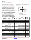
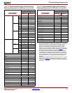
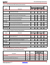
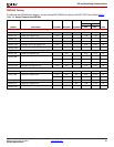
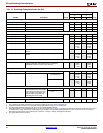
DC and Switching Characteristics
DS610-3 (v2.0) July 16, 2007 www.xilinx.com 35
Product Specification
R
LVCMOS15 Slow 2
55 55
4
31 31
6
18 18
8
–15
12
–10
Fast 2
25 25
4
10 10
6
66
8
–4
12
–3
QuietIO 2
70 70
4
40 40
6
31 31
8
–31
12
–20
LVCMOS12 Slow 2
40 40
4
–25
6
–18
Fast 2
31 31
4
–13
6
–9
QuietIO 2
55 55
4
–36
6
–36
PCI33_3
16 16
PCI66_3
–13
PCIX
–11
HSTL_I
–20
HSTL_III
–8
HSTL_I_18
17 17
HSTL_II_18
–5
HSTL_III_18
10 8
SSTL18_I
715
SSTL18_II
–3
SSTL2_I
18 18
SSTL2_II
–9
SSTL3_I
810
SSTL3_II
67
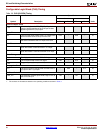
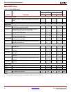
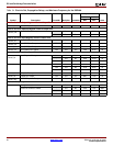
Differential Standards (Number of I/O Pairs or Channels)
LVDS_ 25
22
–
LVDS_ 33
27
–
BLVDS_25
44
MINI_LVDS_25
22
–
MINI_LVDS_33
27
–
LVPECL_25
Inputs Only
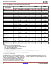
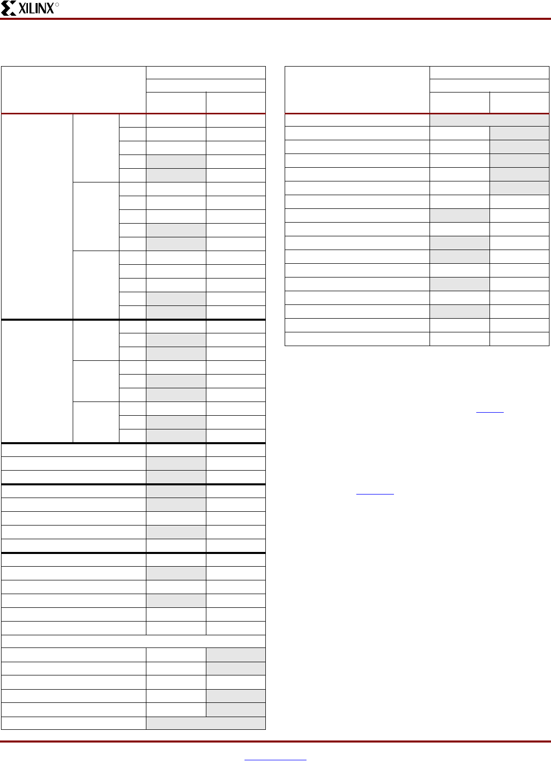
Table 27:
Recommended Number of Simultaneously
Switching Outputs per V
CCO
-GND Pair (V
CCAUX
=3.3V)
Signal Standard
(IOSTANDARD)
Package Type
CS484, FG676
Top, Bottom
(Banks 0,2)
Left, Right
(Banks 1,3)
LVPECL_33
Inputs Only
RSDS_25
22
–
RSDS_33
27
–
TMDS_33
27
–
PPDS_25
22
–
PPDS_33
27
–
DIFF_HSTL_I_18
88
DIFF_HSTL_II_18
–2
DIFF_HSTL_III_18
54
DIFF_HSTL_I
–10
DIFF_HSTL_III
–4
DIFF_SSTL18_I
37
DIFF_SSTL18_II
–1
DIFF_SSTL2_I
99
DIFF_SSTL2_II
–4
DIFF_SSTL3_I
45
DIFF_SSTL3_II
33
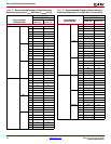
Notes:
1. Not all I/O standards are supported on all I/O banks. The left and
right banks (I/O banks 1 and 3) support higher output drive
current than the top and bottom banks (I/O banks 0 and 2).
Similarly, true differential output standards, such as LVDS,
RSDS, PPDS, miniLVDS, and TMDS, are only supported in top
or bottom banks (I/O banks 0 and 2). Refer to UG331
:
Spartan-3
Generation FPGA User Guide
for additional information.
2. The numbers in this table are recommendations that assume
sound board lay out practice. This table assumes the following
parasitic factors: combined PCB trace and land inductance per
V
CCO
and GND pin of 1.0 nH, receiver capacitive load of 15 pF.
Test limits are the V
IL
/V
IH
voltage limits for the respective I/O
standard.
3. If more than one signal standard is assigned to the I/Os of a given
bank, refer to XAPP689
:
Managing Ground Bounce in Large
FPGAs
for information on how to perform weighted average SSO
calculations.
Table 27:
Recommended Number of Simultaneously
Switching Outputs per V
CCO
-GND Pair (V
CCAUX
=3.3V)
Signal Standard
(IOSTANDARD)
Package Type
CS484, FG676
Top, Bottom
(Banks 0,2)
Left, Right
(Banks 1,3)