


DC and Switching Characteristics
16 www.xilinx.com DS610-3 (v2.0) July 16, 2007
Product Specification
R
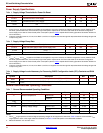
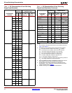
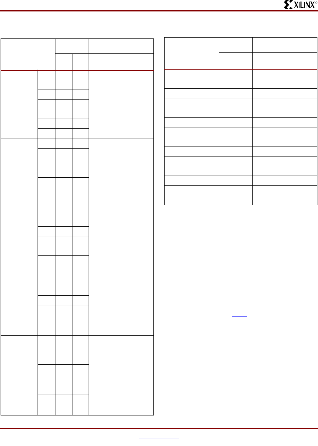
Table 11:
DC Characteristics of User I/Os Using
Single-Ended Standards
IOSTANDARD
Attribute
Test
Conditions
Logic Level
Characteristics
I
OL
(mA)
I
OH
(mA)
V
OL
Max (V)
V
OH
Min (V)
LVTTL
(3)
22–2 0.4 2.4
44–4
66–6
88–8
12 12 –12
16 16 –16
24 24 –24
LVCMOS33
(3)
22–2 0.4 V
CCO
– 0.4
44–4
66–6
88–8
12 12 –12
16 16 –16
24
(4)
24 –24
LVCMOS25
(3)
22–2 0.4 V
CCO
– 0.4
44–4
66–6
88–8
12 12 –12
16
(4)
16 –16
24
(4)
24 –24
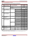
LVCMOS18
(3)
2 2 –2 0.45 V
CCO
– 0.45
44–4
66–6
88–8
12
(4)
12 –12
16
(4)
16 –16
LVCMOS15
(3)
2 2 –2 0.25 • V
CCO
0.75 • V
CCO
44–4
66–6
8
(4)
8–8
12
(4)
12 –12
LVCMOS12
(3)
22–2 0.4 V
CCO
– 0.4
4
(4)
4–4
6
(4)
6–6
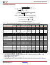
PCI33_3
(5)
1.5 –0.5 10% V
CCO
90% V
CCO
PCI66_3
(5)
1.5 –0.5 10% V
CCO
90% V
CCO
PCIX 1.5 –0.5 10% V
CCO
90% V
CCO
HSTL_I
(4)
8–8 0.4 V
CCO
- 0.4
HSTL_III
(4)
24 –8 0.4 V
CCO
- 0.4
HSTL_I_18 8 –8 0.4 V
CCO
- 0.4
HSTL_II_18
(4)
16 –16 0.4 V
CCO
- 0.4
HSTL_III_18 24 –8 0.4 V
CCO
- 0.4
SSTL18_I 6.7 –6.7
V
TT
– 0.475 V
TT
+ 0.475
SSTL18_II
(4)
13.4 –13.4
V
TT
– 0.475 V
TT
+ 0.475
SSTL2_I 8.1 –8.1 V
TT
– 0.61 V
TT
+ 0.61
SSTL2_II
(4)
16.2 –16.2 V
TT
– 0.80 V
TT
+ 0.80
SSTL3_I 8 –8 V
TT
– 0.6 V
TT
+ 0.6
SSTL3_II
(4)
16 –16 V
TT
– 0.8 V
TT
+ 0.8
Notes:
1. The numbers in this table are based on the conditions set forth in
Table 7 and Table 10.
2. Descriptions of the symbols used in this table are as follows:
I
OL
– the output current condition under which V
OL
is tested
I
OH
– the output current condition under which V
OH
is tested
V
OL
– the output voltage that indicates a Low logic level
V
OH
– the output voltage that indicates a High logic level
V
IL
– the input voltage that indicates a Low logic level
V
IH
– the input voltage that indicates a High logic level
V
CCO
– the supply voltage for output drivers
V
REF
– the reference voltage for setting the input switching threshold
V
TT
– the voltage applied to a resistor termination
3. For the LVCMOS and LVTTL standards: the same V
OL
and V
OH
limits apply for both the Fast and Slow slew attributes.
4. These higher-drive output standards are supported only on
FPGA banks 1 and 3. Inputs are unrestricted. See the chapter
"Using I/O Resources" in UG331
.
5. Tested according to the relevant PCI specifications.
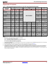
Table 11:
DC Characteristics of User I/Os Using
Single-Ended Standards
(Continued)
IOSTANDARD
Attribute
Test
Conditions
Logic Level
Characteristics
I
OL
(mA)
I
OH
(mA)
V
OL
Max (V)
V
OH
Min (V)