


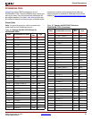
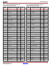
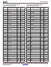

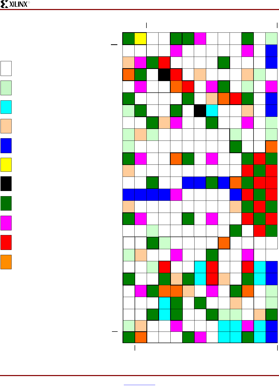
Pinout Descriptions
DS610-4 (v2.0) July 16, 2007 www.xilinx.com 93
Product Specification
R
FG676 Footprint -
XC3SD3400A FPGA
Left Half of Package (top
view)
314
I/O: Unrestricted,
general-purpose user I/O.
34
INPUT: Unrestricted,
general-purpose input pin.
52
DUAL: Configuration,
AWAKE pins, then possible
user I/O.
37
VREF: User I/O or input
voltage reference for bank.
32
CLK: User I/O, input, or
clock buffer input.
3
CONFIG: Dedicated
configuration pins
,
SUSPEND pin.
4
JTAG: Dedicated JTAG
port pins.
100
GND: Ground
40
VCCO: Output voltage
supply for bank.
36
VCCINT: Internal core
supply voltage (+1.2V).
24
VCCAUX: Auxiliary supply
voltage.
Note:
The boxes with
question marks inside
indicate pin differences
from the XC3SD1800A
device. Please see the
"Footprint Migration
Differences" section for
more information.
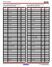
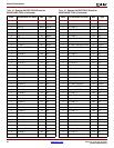
Figure 18:
FG676 Package Footprint for XC3SD3400A FPGA (top view)
12345678910111213
A
GND
PROG_
B
I/O
L51P_0
I/O
L45P_0
GND
∇
GND
VCCO_0
∇
I/O
L38P_0
I/O
L36P_0
I/O
L33P_0
GND
I/O
L29P_0
INPUT
B
I/O
L02N_3
I/O
L02P_3
I/O
L51N_0
I/O
L45N_0
VCCO_0
I/O
L41P_0
I/O
L42P_0
I/O
L38N_0
I/O
L36N_0
I/O
L33N_0
VCCO_0
I/O
L29N_0
I/O
L28P_0
GCLK10
C
INPUT
VREF_3
∇
VCCO_3
∇
GND
VCCINT
∇
I/O
L44P_0
I/O
L41N_0
I/O
L42N_0
I/O
L40P_0
GND
I/O
L34P_0
I/O
L32P_0
I/O
L30N_0
I/O
L28N_0
GCLK11
D
VCCAUX
∇
GND
∇
I/O
L06P_3
TMS
VCCINT
∇
I/O
L44N_0
INPUT
VREF_0
I/O
L40N_0
I/O
L37N_0
I/O
L34N_0
I/O
L32N_0
VREF_0
INPUT
I/O
L30P_0
E
I/O
L11P_3
VCCO_3
I/O
L07P_3
I/O
L06N_3
VCCAUX
VCCINT
∇
I/O
L48N_0
VCCO_0
GND
∇
I/O
L37P_0
INPUT
I/O
L31P_0
VCCO_0
F
GND
I/O
L11N_3
I/O
L14N_3
I/O
L07N_3
I/O
L09P_3
GND
I/O
L48P_0
I/O
L52P_0
VREF_0
VCCAUX
∇
VCCINT
∇
GND
I/O
L31N_0
I/O
L27P_0
GCLK8
G
INPUT
∇
GND
∇
I/O
L14P_3
I/O
L09N_3
GND
∇
I/O
L03P_3
TDI
I/O
L52N_0
PUDC_B
I/O
L47P_0
I/O
L46P_0
INPUT
VREF_0
I/O
L35P_0
I/O
L27N_0
GCLK9
H
I/O
L17N_3
I/O
L17P_3
GND
INPUT
VREF_3
∇
VCCO_3
I/O
L10N_3
I/O
L03N_3
GND
I/O
L47N_0
I/O
L46N_0
VCCO_0
I/O
L35N_0
INPUT
J
INPUT
L24P_3
INPUT
L20N_3
VREF_3
INPUT
L20P_3
I/O
L19N_3
I/O
L19P_3
I/O
L13N_3
I/O
L10P_3
I/O
L01P_3
I/O
L01N_3
INPUT
I/O
L43P_0
I/O
L39P_0
INPUT
K
INPUT
L24N_3
I/O
L23N_3
I/O
L23P_3
I/O
L22N_3
I/O
L22P_3
I/O
L18P_3
I/O
L13P_3
I/O
L05N_3
I/O
L05P_3
GND
I/O
L43N_0
I/O
L39N_0
VCCAUX
L
GND
VCCO_3
I/O
L25N_3
I/O
L25P_3
VCCAUX
GND
I/O
L18N_3
VCCO_3
I/O
L15N_3
I/O
L15P_3
GND VCCINT GND
M
I/O
L29N_3
VREF_3
I/O
L29P_3
I/O
L27N_3
I/O
L27P_3
I/O
L28P_3
I/O
L28N_3
I/O
L26N_3
I/O
L26P_3
I/O
L21N_3
I/O
L21P_3
VCCINT GND VCCINT
N
I/O
L31P_3
I/O
L31N_3
GND
I/O
L30N_3
I/O
L30P_3
I/O
L32P_3
LHCLK0
I/O
L32N_3
LHCLK1
GND
I/O
L35P_3
TRDY2
LHCLK6
VCCAUX
GND VCCINT VCCINT
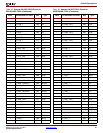
P
I/O
L33P_3
LHCLK2
I/O
L33N_3
IRDY2
LHCLK3
I/O
L34N_3
LHCLK5
I/O
L34P_3
LHCLK4
VCCO_3
I/O
L39N_3
I/O
L39P_3
I/O
L41P_3
I/O
L41N_3
I/O
L35N_3
LHCLK7
VCCINT GND VCCINT
R
I/O
L36P_3
VREF_3
I/O
L36N_3
I/O
L37P_3
I/O
L37N_3
I/O
L40P_3
I/O
L40N_3
I/O
L45N_3
I/O
L45P_3
I/O
L43N_3
I/O
L43P_3
VREF_3
GND VCCINT GND
T
GND
VCCO_3
I/O
L38P_3
I/O
L38N_3
I/O
L42P_3
GND
I/O
L51P_3
VCCO_3
I/O
L48N_3
I/O
L48P_3
VCCINT GND VCCINT
U
I/O
L44P_3
I/O
L44N_3
INPUT
L46P_3
I/O
L42N_3
I/O
L49P_3
I/O
L51N_3
I/O
L56P_3
I/O
L56N_3
I/O
L61P_3
GND
I/O
L13N_2
VCCINT GND
Bank 0
Bank 3
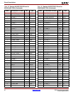
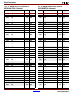
V
I/O
L47P_3
I/O
L47N_3
GND
INPUT
L46N_3
I/O
L49N_3
I/O
L59N_3
I/O
L59P_3
I/O
L61N_3
VCCAUX
I/O
L09P_2
I/O
L13P_2
I/O
L16P_2
I/O
L20P_2
W
INPUT
L50P_3
INPUT
L50N_3
VREF_3
I/O
L52P_3
I/O
L52N_3
VCCO_3
I/O
L63N_3
I/O
L63P_3
GND
I/O
L05P_2
I/O
L09N_2
VCCO_2
I/O
L16N_2
I/O
L20N_2
Y
I/O
L53P_3
I/O
L53N_3
INPUT
∇
VCCINT
∇
I/O
L57P_3
I/O
L57N_3
I/O
L02P_2
M2
VCCINT
∇
I/O
L05N_2
I/O
L12P_2
VCCINT
∇
I/O
L17P_2
RDWR_B
I/O
L25N_2
GCLK13
A
A
GND
I/O
L55P_3
I/O
L55N_3
GND
∇
INPUT
VREF_3
∇
GND
I/O
L02N_2
CSO_B
VCCINT
∇
INPUT
VREF_2
I/O
L12N_2
GND
I/O
L17N_2
VS2
I/O
L25P_2
GCLK12
A
B
I/O
L60P_3
VCCO_3
GND
∇
VCCAUX
∇
VCCAUX
INPUT
VREF_2
I/O
L14N_2
VCCO_2
I/O
L15P_2
GND
∇
VCCAUX
I/O
L21P_2
INPUT
A
C
I/O
L60N_3
I/O
L64P_3
I/O
L64N_3
I/O
L01P_2
M1
GND
∇
I/O
L08P_2
GND
∇
I/O
L14P_2
I/O
L15N_2
INPUT
VREF_2
I/O
L23N_2
I/O
L21N_2
INPUT
A
D
I/O
L65P_3
I/O
L65N_3
GND
I/O
L01N_2
M0
GND
∇
I/O
L08N_2
I/O
L11P_2
GND
INPUT INPUT
I/O
L23P_2
INPUT
VREF_2
GND
A
E
INPUT
L66P_3
INPUT
L66N_3
VREF_3
I/O
L06P_2
I/O
L07P_2
VCCO_2
I/O
L10N_2
I/O
L11N_2
I/O
L18P_2
I/O
L19P_2
VS1
I/O
L22P_2
D7
VCCO_2
I/O
L24N_2
D4
I/O
L26N_2
GCLK15
A
F
GND
VCCAUX
∇
I/O
L06N_2
I/O
L07N_2
I/O
L10P_2
GND
VCCO_2
∇
I/O
L18N_2
I/O
L19N_2
VS0
I/O
L22N_2
D6
GND
I/O
L24P_2
D5
I/O
L26P_2
GCLK14
Bank 2