


DC and Switching Characteristics
32 www.xilinx.com DS610-3 (v2.0) July 16, 2007
Product Specification
R
The capacitive load (C
L
) is connected between the output
and GND.
The Output timing for all standards, as published
in the speed files and the data sheet, is always based on a
C
L
value of zero.
High-impedance probes (less than 1 pF)
are used for all measurements. Any delay that the test
fixture might contribute to test measurements is subtracted
from those measurements to produce the final timing
numbers as published in the speed files and data sheet.
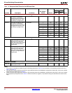
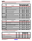
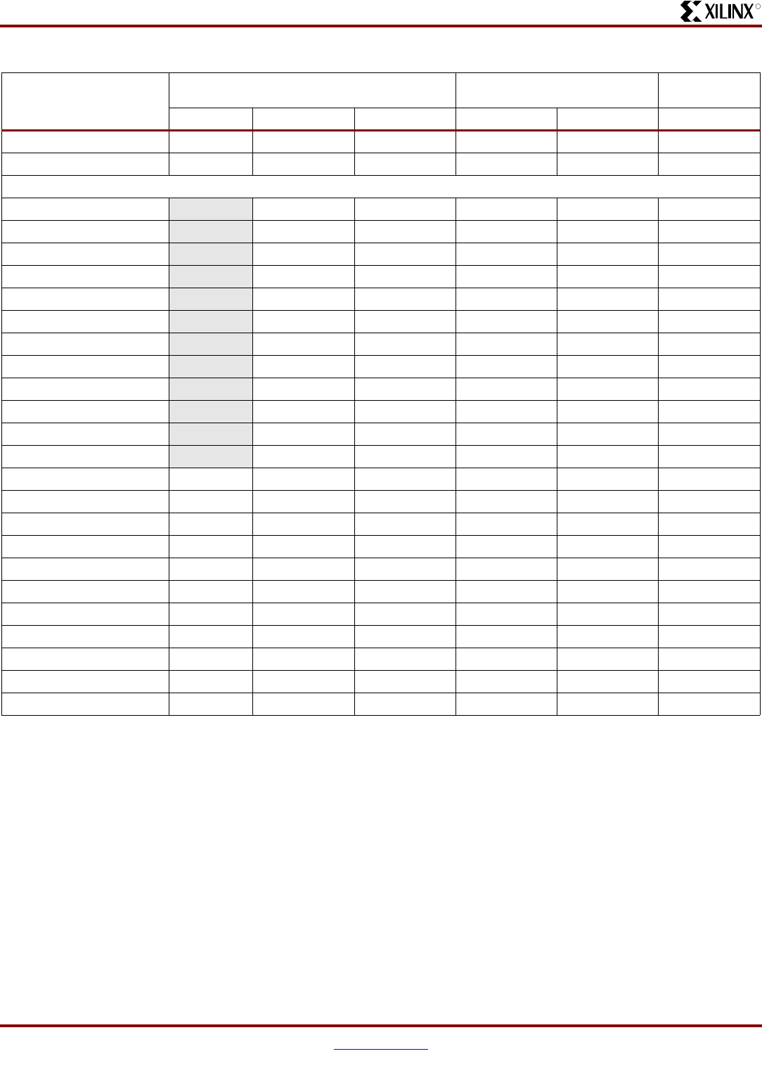
SSTL3_I 1.5 V
REF
– 0.75 V
REF
+ 0.75 50 1.5 V
REF
SSTL3_II 1.5 V
REF
– 0.75 V
REF
+ 0.75 25 1.5 V
REF
Differential
LVDS_25 -V
ICM
– 0.125 V
ICM
+ 0.125 50 1.2 V
ICM
LVDS_33 -V
ICM
– 0.125 V
ICM
+ 0.125 50 1.2 V
ICM
BLVDS_25 -V
ICM
– 0.125 V
ICM
+ 0.125 1M 0 V
ICM
MINI_LVDS_25 -V
ICM
– 0.125 V
ICM
+ 0.125 50 1.2 V
ICM
MINI_LVDS_33 -V
ICM
– 0.125 V
ICM
+ 0.125 50 1.2 V
ICM
LVPECL_25 -V
ICM
– 0.3 V
ICM
+ 0.3 N/A N/A V
ICM
LVPECL_33 -V
ICM
– 0.3 V
ICM
+ 0.3 N/A N/A V
ICM
RSDS_25 -V
ICM
– 0.1 V
ICM
+ 0.1 50 1.2 V
ICM
RSDS_33 -V
ICM
– 0.1 V
ICM
+ 0.1 50 1.2 V
ICM
TMDS_33 -V
ICM
– 0.1 V
ICM
+ 0.1 50 3.3 V
ICM
PPDS_25 -V
ICM
– 0.1 V
ICM
+ 0.1 50 0.8 V
ICM
PPDS_33 -V
ICM
– 0.1 V
ICM
+ 0.1 50 0.8 V
ICM
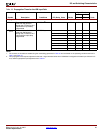
DIFF_HSTL_I_18 0.9 V
REF
– 0.5 V
REF
+ 0.5 50 0.9 V
REF
DIFF_HSTL_II_18 0.9 V
REF
– 0.5 V
REF
+ 0.5 50 0.9 V
REF
DIFF_HSTL_III_18 1.1 V
REF
– 0.5 V
REF
+ 0.5 50 1.8 V
REF
DIFF_HSTL_I 0.9 V
REF
– 0.5 V
REF
+ 0.5 50 0.9 V
REF
DIFF_HSTL_III 0.9 V
REF
– 0.5 V
REF
+ 0.5 50 0.9 V
REF
DIFF_SSTL18_I 0.9 V
REF
– 0.5 V
REF
+ 0.5 50 0.9 V
REF
DIFF_SSTL18_II 0.9 V
REF
– 0.5 V
REF
+ 0.5 50 0.9 V
REF
DIFF_SSTL2_I 1.25 V
REF
– 0.5 V
REF
+ 0.5 50 1.25 V
REF
DIFF_SSTL2_II 1.25 V
REF
– 0.5 V
REF
+ 0.5 50 1.25 V
REF
DIFF_SSTL3_I 1.5 V
REF
– 0.5 V
REF
+ 0.5 50 1.5 V
REF
DIFF_SSTL3_II 1.5 V
REF
– 0.5 V
REF
+ 0.5 50 1.5 V
REF
Notes:
1. Descriptions of the relevant symbols are as follows:
V
REF
– The reference voltage for setting the input switching threshold
V
ICM
– The common mode input voltage
V
M
– Voltage of measurement point on signal transition
V
L
– Low-level test voltage at Input pin
V
H
– High-level test voltage at Input pin
R
T
– Effective termination resistance, which takes on a value of 1 MΩ when no parallel termination is required
V
T
– Termination voltage
2. The load capacitance (C
L
) at the Output pin is 0 pF for all signal standards.
3. According to the PCI specification.
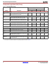
Table 25:
Test Methods for Timing Measurement at I/Os
(Continued)
Signal Standard
(IOSTANDARD)
Inputs Outputs
Inputs and
Outputs
V
REF
(V) V
L
(V) V
H
(V) R
T
(Ω)V
T
(V) V
M
(V)