


DC and Switching Characteristics
DS610-3 (v2.0) July 16, 2007 www.xilinx.com 19
Product Specification
R
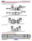
External Termination Requirements for Differential I/O
LVDS, RSDS, MINI_LVDS, and PPDS I/O Standards
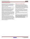
BLVDS_25 I/O Standard
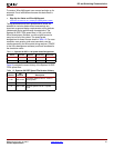
TMDS_33 I/O Standard
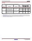
Device DNA Data Retention, Read Endurance
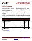
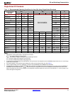
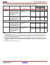
Figure 5:
External Input Termination for LVDS, RSDS, MINI_LVDS, and PPDS I/O Standards
Z0 = 50Ω
Z
0 = 50Ω
100Ω
DS529-3_09_020107
a) Input-only differential pairs or pairs not using DIFF_TERM=Yes constraint
Z0 = 50Ω
Z
0 = 50Ω
b) Differential pairs using DIFF_TERM=Yes constraint
DIFF_TERM=No
DIFF_TERM=Yes
LVDS_33,
MINI_LVDS_33,
RSDS_33,
PPDS_33
LVDS_33, LVDS_25,
MINI_LVDS_33,
MINI_LVDS_25,
RSDS_33, RSDS_25,
PPDS_33, PPDS_25
CAT16-PT4F4
Part Number
/ th of Bourns
1
4
VCCO = 3.3V
LVDS_25,
MINI_LVDS_25,
RSDS_25,
PPDS_25
VCCO = 2.5V
LVDS_33,
MINI_LVDS_33,
RSDS_33,
PPDS_33
VCCO = 3.3V
LVDS_25,
MINI_LVDS_25,
RSDS_25,
PPDS_25
VCCO = 2.5V
No VCCO Restrictions
R
LVDS_33,
MINI_LVDS_33,
RSDS_33,
PPDS_33
VCCO = 3.3V
LVDS_25,
MINI_LVDS_25,
RSDS_25,
PPDS_25
VCCO = 2.5V
DT
Bank 0
Bank 2
Bank 0
Bank 2
Bank 3
Bank 1
Bank 0 and 2 Any Bank
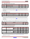
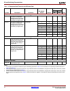
Figure 6:
External Termination Resistors for BLVDS_25 I/O Standard
Z0 = 50Ω
Z
0 = 50Ω
140Ω
165Ω
165Ω
100Ω
VCCO = 2.5V
No VCCO Requirement
DS529-3_07_020107
BLVDS_25
BLVDS_25
CAT16-LV4F12
Part Number
/ th of Bourns
1
4
CAT16-PT4F4
Part Number
/ th of Bourns
1
4
Bank 0
Bank 2
Bank 3
Bank 1
Any Bank
Bank 0
Bank 2
Bank 3
Bank 1
Any Bank
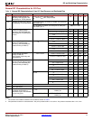
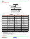
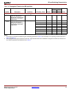
Figure 7:
External Input Resistors Required for TMDS_33 I/O Standard
50Ω
V
CCO
= 3.3V
V
CCAUX
= 3.3V
DS529-3_08_020107DVI/HDMI cable
50Ω
3.3V
TMDS_33 TMDS_33
Bank 0
Bank 2
Bank 0 and 2
Bank 0
Bank 2
Bank 3
Bank 1
Any Bank
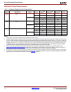
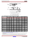
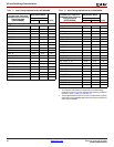
Table 14:
Device DNA Identifier Memory Characteristics
Symbol Description Minimum Units
DNA_RETENTION Data retention, continuous usage 10 Years
DNA_CYCLES
Number of READ operations or JTAG ISC_DNA read operations. Unaffected by
HOLD or SHIFT operations.
30,000,000
Read
cycles