


DC and Switching Characteristics
56 www.xilinx.com DS610-3 (v2.0) July 16, 2007
Product Specification
R
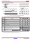
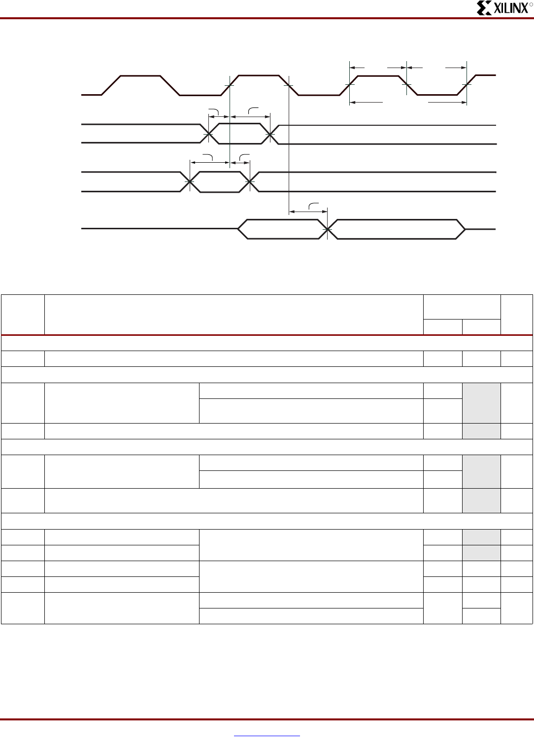
IEEE 1149.1/1553 JTAG Test Access Port Timing
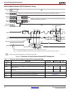
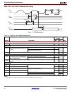
Figure 15:
JTAG Waveforms
TCK
T
TMSTCK
TMS
TDI
TDO
(Input)
(Input)
(Input)
(Output)
T
TCKTMS
T
TCKTDI
T
TCKTDO
T
TDITCK
DS099_06_040703
T
CCH
T
CCL
1/F
TCK
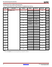
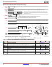
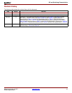
Table 55:
Timing for the JTAG Test Access Port
Symbol Description
All Speed
Grades
UnitsMin Max
Clock-to-Output Times
T
TCKTDO
The time from the falling transition on the TCK pin to data appearing at the TDO pin 1.0 11.0 ns
Setup Times
T
TDITCK
The time from the setup of data at the
TDI pin to the rising transition at the
TCK pin
All functions except those shown below 7.0 –ns
Boundary scan commands
(INTEST, EXTEST, SAMPLE)
13.0
T
TMSTCK
The time from the setup of a logic level at the TMS pin to the rising transition at the TCK pin 7.0 –ns
Hold Times
T
TCKTDI
The time from the rising transition at
the TCK pin to the point when data is
last held at the TDI pin
All functions except those shown below 0 –ns
Configuration commands (CFG_IN, ISC_PROGRAM) 3.5
T
TCKTMS
The time from the rising transition at the TCK pin to the point when a logic level is last held at the
TMS pin
0 –ns
Clock Timing
T
CCH
The High pulse width at the TCK pin All functions except ISC_DNA command 5 –ns
T
CCL
The Low pulse width at the TCK pin 5 –ns
T
CCHDNA
The High pulse width at the TCK pin During ISC_DNA command 10 10,000 ns
T
CCLDNA
The Low pulse width at the TCK pin 10 10,000 ns
F
TCK
Frequency of the TCK signal BYPASS or HIGHZ instructions 0 33 MHz
All operations except for BYPASS or HIGHZ instructions 20
Notes:
1. The numbers in this table are based on the operating conditions set forth in Table 7.