


DC and Switching Characteristics
DS610-3 (v2.0) July 16, 2007 www.xilinx.com 43
Product Specification
R
Digital Frequency Synthesizer (DFS)
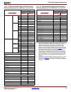
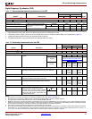
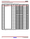
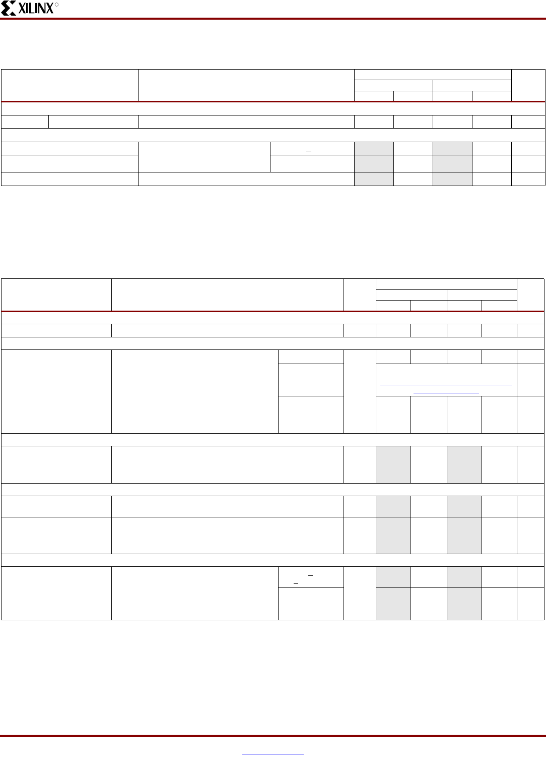
Table 37:
Recommended Operating Conditions for the DFS
Symbol Description
Speed Grade
Units
-5 -4
Min Max Min Max
Input Frequency Ranges
(2)
F
CLKIN
CLKIN_FREQ_FX Frequency for the CLKIN input 0.2 333 0.2 333 MHz
Input Clock Jitter Tolerance
(3)
CLKIN_CYC_JITT_FX_LF Cycle-to-cycle jitter at the CLKIN
input, based on CLKFX output
frequency
F
CLKFX
< 150 MHz - ±300 -±300ps
CLKIN_CYC_JITT_FX_HF F
CLKFX
> 150 MHz - ±150 -±150ps
CLKIN_PER_JITT_FX Period jitter at the CLKIN input
-±1-±1ns
Notes:
1. DFS specifications apply when either of the DFS outputs (CLKFX or CLKFX180) are used.
2. If both DFS and DLL outputs are used on the same DCM, follow the more restrictive CLKIN_FREQ_DLL specifications in Table 35.
3. CLKIN input jitter beyond these limits may cause the DCM to lose lock.
4. The DCM specifications are guaranteed when both adjacent DCMs are locked
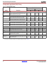
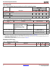
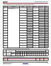
Table 38:
Switching Characteristics for the DFS
Symbol Description Device
Speed Grade
Units
-5 -4
Min Max Min Max
Output Frequency Ranges
CLKOUT_FREQ_FX
(2)
Frequency for the CLKFX and CLKFX180 outputs All 5 350 5 311 MHz
Output Clock Jitter
(3,4)
CLKOUT_PER_JITT_FX Period jitter at the CLKFX and CLKFX180
outputs.
All Typ Max Typ Max
CLKIN
≤ 20 MHz
Use the Spartan-3A Jitter Calculator:
www.xilinx.com/bvdocs/publications/
s3a_jitter_calc.zip
ps
CLKIN
> 20 MHz
±[1% of
CLKFX
period
+ 100]
±[1% of
CLKFX
period
+ 200]
±[1% of
CLKFX
period
+ 100]
±[1% of
CLKFX
period
+ 200]
ps
Duty Cycle
(5,6)
CLKOUT_DUTY_CYCLE_FX Duty cycle precision for the CLKFX and CLKFX180 outputs,
including the BUFGMUX and clock tree duty-cycle distortion
All -±[1% of
CLKFX
period
+ 350]
-±[1% of
CLKFX
period
+ 350]
ps
Phase Alignment
(6)
CLKOUT_PHASE_FX Phase offset between the DFS CLKFX output and the DLL CLK0
output when both the DFS and DLL are used
All - ±200 - ±200 ps
CLKOUT_PHASE_FX180 Phase offset between the DFS CLKFX180 output and the DLL
CLK0 output when both the DFS and DLL are used
All -±[1% of
CLKFX
period
+ 200]
-±[1% of
CLKFX
period
+ 200]
ps
Lock Time
LOCK_FX
(2,3)
The time from deassertion at the DCM’s
Reset input to the rising transition at its
LOCKED output. The DFS asserts LOCKED
when the CLKFX and CLKFX180 signals are
valid. If using both the DLL and the DFS, use
the longer locking time.
5 MHz <
F
CLKIN
<
15 MHz
All
-5-5ms
F
CLKIN
> 15 MHz - 450 - 450 μs
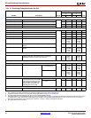
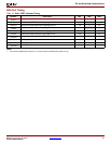
Notes:
1. The numbers in this table are based on the operating conditions set forth in Table 7 and Table 37.
2. DFS performance requires the additional logic automatically added by ISE 9.1i and later software revisions.
3. For optimal jitter tolerance and faster lock time, use the CLKIN_PERIOD attribute.
4. Maximum output jitter is characterized within a reasonable noise environment (40 SSOs and 25% CLB switching) on an FPGA. Output jitter strongly
depends on the environment, including the number of SSOs, the output drive strength, CLB utilization, CLB switching activities, switching frequency,
power supply and PCB design. The actual maximum output jitter depends on the system application.
5. The CLKFX and CLKFX180 outputs always have an approximate 50% duty cycle.
6. Some duty-cycle and alignment specifications include a percentage of the CLKFX output period. For example, the data sheet specifies a maximum
CLKFX jitter of “±[1% of CLKFX period + 200]”. Assume the CLKFX output frequency is 100 MHz. The equivalent CLKFX period is 10 ns and 1% of
10 ns is 0.1 ns or 100 ps. According to the data sheet, the maximum jitter is ±[100 ps + 200 ps] = ±300 ps.