


DC and Switching Characteristics
36 www.xilinx.com DS610-3 (v2.0) July 16, 2007
Product Specification
R
Configurable Logic Block (CLB) Timing
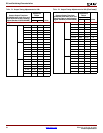
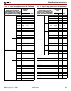
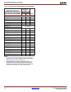
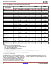
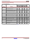
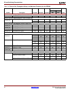
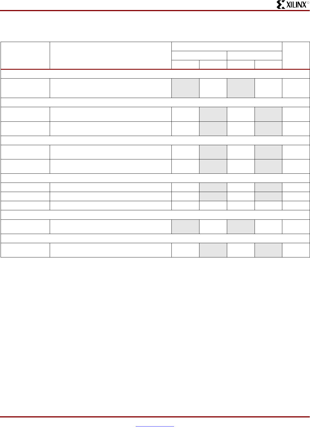
Table 28:
CLB (SLICEM) Timing
Symbol Description
Speed Grade
Units
-5 -4
Min Max Min Max
Clock-to-Output Times
T
CKO
When reading from the FFX (FFY) Flip-Flop, the time
from the active transition at the CLK input to data
appearing at the XQ (YQ) output
–0.60–0.68ns
Setup Times
T
AS
Time from the setup of data at the F or G input to the
active transition at the CLK input of the CLB
0.18 –0.36–ns
T
DICK
Time from the setup of data at the BX or BY input to
the active transition at the CLK input of the CLB
1.58 –1.88–ns
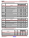
Hold Times
T
AH
Time from the active transition at the CLK input to the
point where data is last held at the F or G input
0.00 –0.00–ns
T
CKDI
Time from the active transition at the CLK input to the
point where data is last held at the BX or BY input
0.00 –0.00–ns
Clock Timing
T
CH
The High pulse width of the CLB’s CLK signal 0.63 –0.75–ns
T
CL
The Low pulse width of the CLK signal 0.63 –0.75–ns
F
TOG
Toggle frequency (for export control) 0 770 0 667 MHz
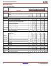
Propagation Times
T
ILO
The time it takes for data to travel from the CLB’s F
(G) input to the X (Y) output
–0.62–0.71ns
Set/Reset Pulse Width
T
RPW_CLB
The minimum allowable pulse width, High or Low, to
the CLB’s SR input
1.33 –1.61–ns
Notes:
1. The numbers in this table are based on the operating conditions set forth in Table 7.