


DS610-4 (v2.0) July 16, 2007 www.xilinx.com 59
Product Specification
© 2007 Xilinx, Inc. All rights reserved. All Xilinx trademarks, registered trademarks, patents, and disclaimers are as listed at http://www.xilinx.com/legal.htm.
All other trademarks are the property of their respective owners. All specifications are subject to change without notice.
Introduction
This section describes how the various pins on a
Spartan™-3A DSP FPGA connect within the supported
component packages and provides device-specific thermal
characteristics. For general information on the pin functions
and the package characteristics, see the
Packaging
section
in:
• UG331: Spartan-3 Generation FPGA User Guide
http://www.xilinx.com/bvdocs/userguides/ug331.pdf
Spartan-3A DSP FPGAs are available in both standard and
Pb-free, RoHS versions of each package, with the Pb-free
version adding a “G” to the middle of the package code.
Except for the thermal characteristics, all information for the
standard package applies equally to the Pb-free package.
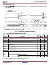
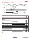
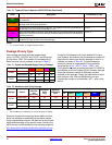
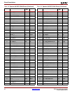
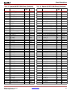
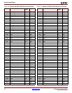
Pin Types
Most pins on a Spartan-3A DSP FPGA are
general-purpose, user-defined I/O pins. There are,
however, up to 12 different functional types of pins on
Spartan-3A DSP packages, as outlined in Table 56. In the
package footprint drawings that follow, the individual pins
are color-coded according to pin type as in the table.
<BL
Blue
>
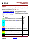
Spartan-3A DSP FPGA Family:
Pinout Descriptions
DS610-4 (v2.0) July 16, 2007
0
Product Specification
R
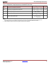
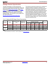
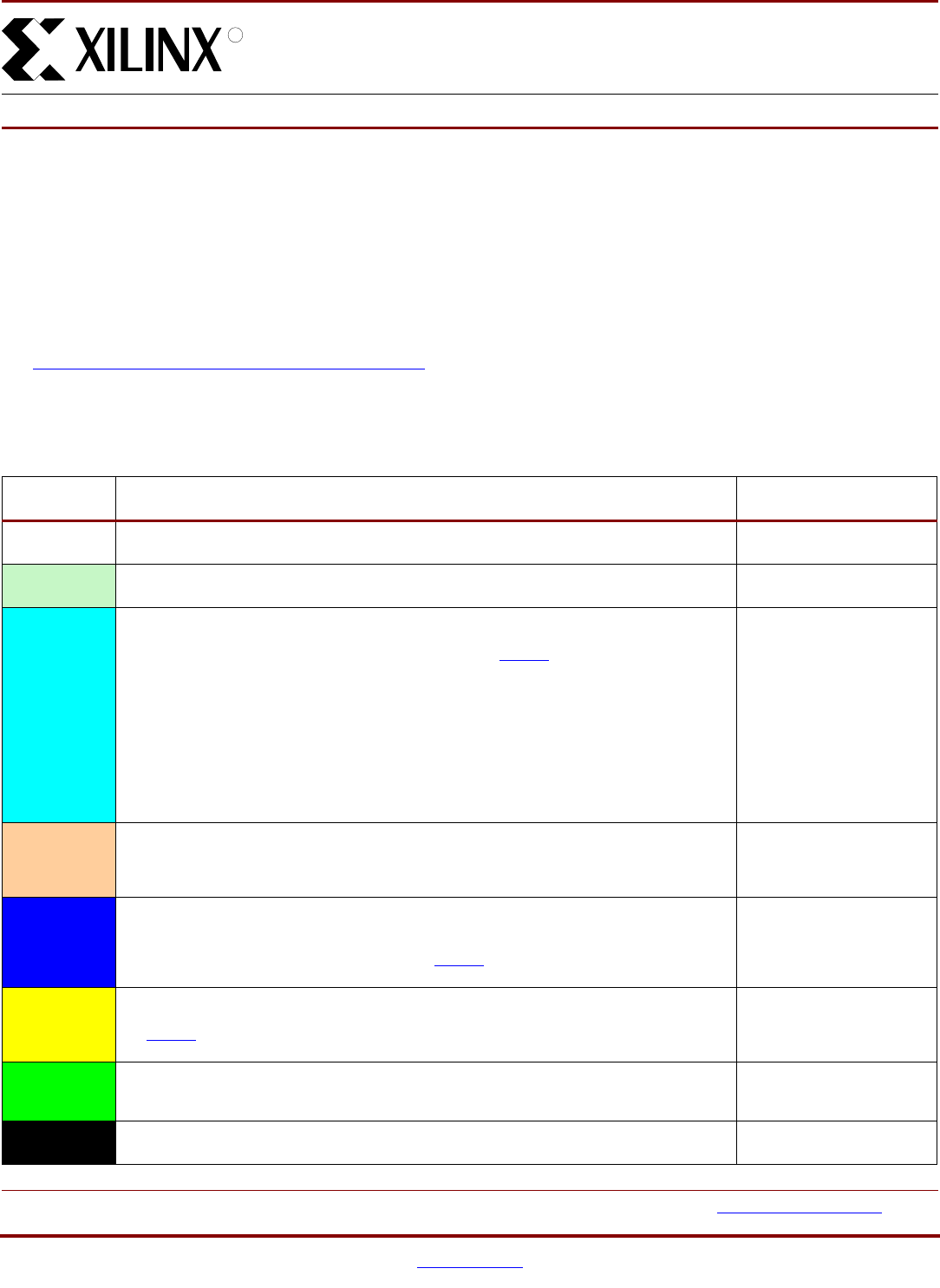
Table 56:
Types of Pins on Spartan-3A DSP FPGAs
Type/Color
Code
Description Pin Name(s) in Type
I/O
Unrestricted, general-purpose user-I/O pin. Most pins can be paired together to form
differential I/Os.
IO_#
IO_Lxxy_#
INPUT
Unrestricted, general-purpose input-only pin. This pin does not have an output structure
or PCI clamp diode.
IP_#
IP_Lxxy_#
DUAL
Dual-purpose pin used in some configuration modes during the configuration process and
then usually available as a user I/O after configuration. If the pin is not used during
configuration, this pin behaves as an I/O-type pin. See UG332:
Spartan-3 Generation
Configuration User Guide
for additional information on these signals.
M[2:0]
PUDC_B
CCLK
MOSI/CSI_B
D[7:1]
D0/DIN
CSO_B
RDWR_B
INIT_B
A[25:0]
VS[2:0]
LDC[2:0]
HDC
VREF
Dual-purpose pin that is either a user-I/O pin or Input-only pin, or, along with all other
VREF pins in the same bank, provides a reference voltage input for certain I/O standards.
If used for a reference voltage within a bank, all VREF pins within the bank must be
connected.
IP/VREF_#
IP_Lxxy_#/VREF_#
IO/VREF_#
IO_Lxxy_#/VREF_#
CLK
Either a user-I/O pin or an input to a specific clock buffer driver. Packages have 16 global
clock inputs that optionally clock the entire device. The RHCLK inputs optionally clock the
right half of the device. The LHCLK inputs optionally clock the left half of the device. See
the Using Global Clock Resources chapter in UG331:
Spartan-3 Generation FPGA User
Guide
for additional information on these signals.
IO_Lxxy_#/GCLK[15:0],
IO_Lxxy_#/LHCLK[7:0],
IO_Lxxy_#/RHCLK[7:0]
CONFIG
Dedicated configuration pin, two per device. Not available as a user-I/O pin. Every
package has two dedicated configuration pins. These pins are powered by VCCAUX. See
the UG332:
Spartan-3 Generation Configuration User Guide
for additional information on
the DONE and PROG_B signals.
DONE, PROG_B
PWR
MGMT
Control and status pins for the power-saving Suspend mode. SUSPEND is a dedicated
pin. AWAKE is a Dual-Purpose pin. Unless Suspend mode is enabled in the application,
AWAKE is available as a user-I/O pin.
SUSPEND, AWAKE
JTAG
Dedicated JTAG pin - 4 per device. Not available as a user-I/O pin. Every package has
four dedicated JTAG pins. These pins are powered by VCCAUX.
TDI, TMS, TCK, TDO