


DC and Switching Characteristics
50 www.xilinx.com DS610-3 (v2.0) July 16, 2007
Product Specification
R
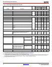
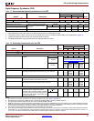
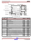
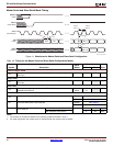
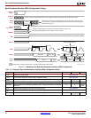
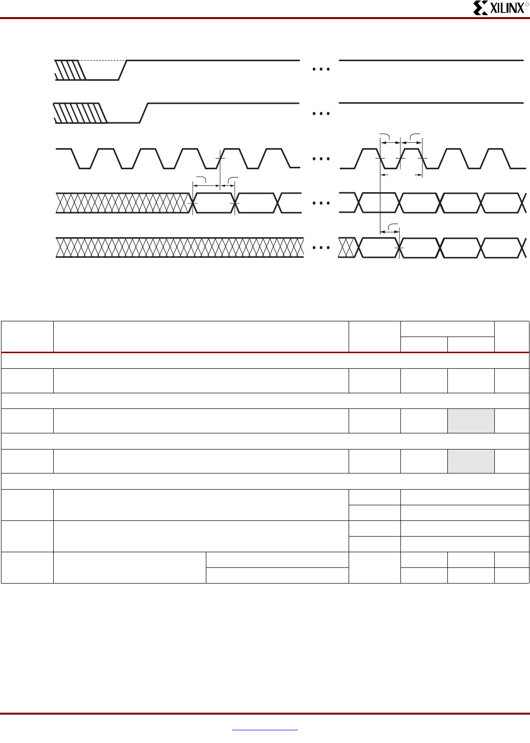
Master Serial and Slave Serial Mode Timing
Figure 11:
Waveforms for Master Serial and Slave Serial Configuration
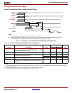
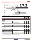
Table 49:
Timing for the Master Serial and Slave Serial Configuration Modes
Symbol Description
Slave/
Master
All Speed Grades
UnitsMin Max
Clock-to-Output Times
T
CCO
The time from the falling transition on the CCLK pin to data appearing at the
DOUT pin
Both 1.5 10 ns
Setup Times
T
DCC
The time from the setup of data at the DIN pin to the rising transition at the
CCLK pin
Both 7 -ns
Hold Times
T
CCD
The time from the rising transition at the CCLK pin to the point when data is
last held at the DIN pin
Master
Slave
0.0
1.0
-ns
Clock Timing
T
CCH
High pulse width at the CCLK input pin Master See Table 47
Slave See Table 48
T
CCL
Low pulse width at the CCLK input pin Master See Table 47
Slave See Table 48
F
CCSER
Frequency of the clock signal at the
CCLK input pin
No bitstream compression Slave 0 100 MHz
With bitstream compression 0 100 MHz
Notes:
1. The numbers in this table are based on the operating conditions set forth in Table 7.
2. For serial configuration with a daisy-chain of multiple FPGAs, the maximum limit is 25 MHz.
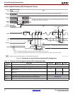
DS312-3_05_103105
Bit 0 Bit 1
Bit n
Bit n+1
Bit n-64
Bit n-63
1/F
CCSER
T
SCCL
T
DCC
T
CCD
T
SCCH
T
CCO
PROG_B
(Input)
DIN
(Input)
DOUT
(Output)
(Open-Drain)
INIT_B
(Input/Output)
CCLK
T
MCCL
T
MCCH