


DC and Switching Characteristics
DS610-3 (v2.0) July 16, 2007 www.xilinx.com 17
Product Specification
R
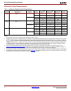
Differential I/O Standards
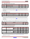
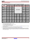
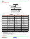
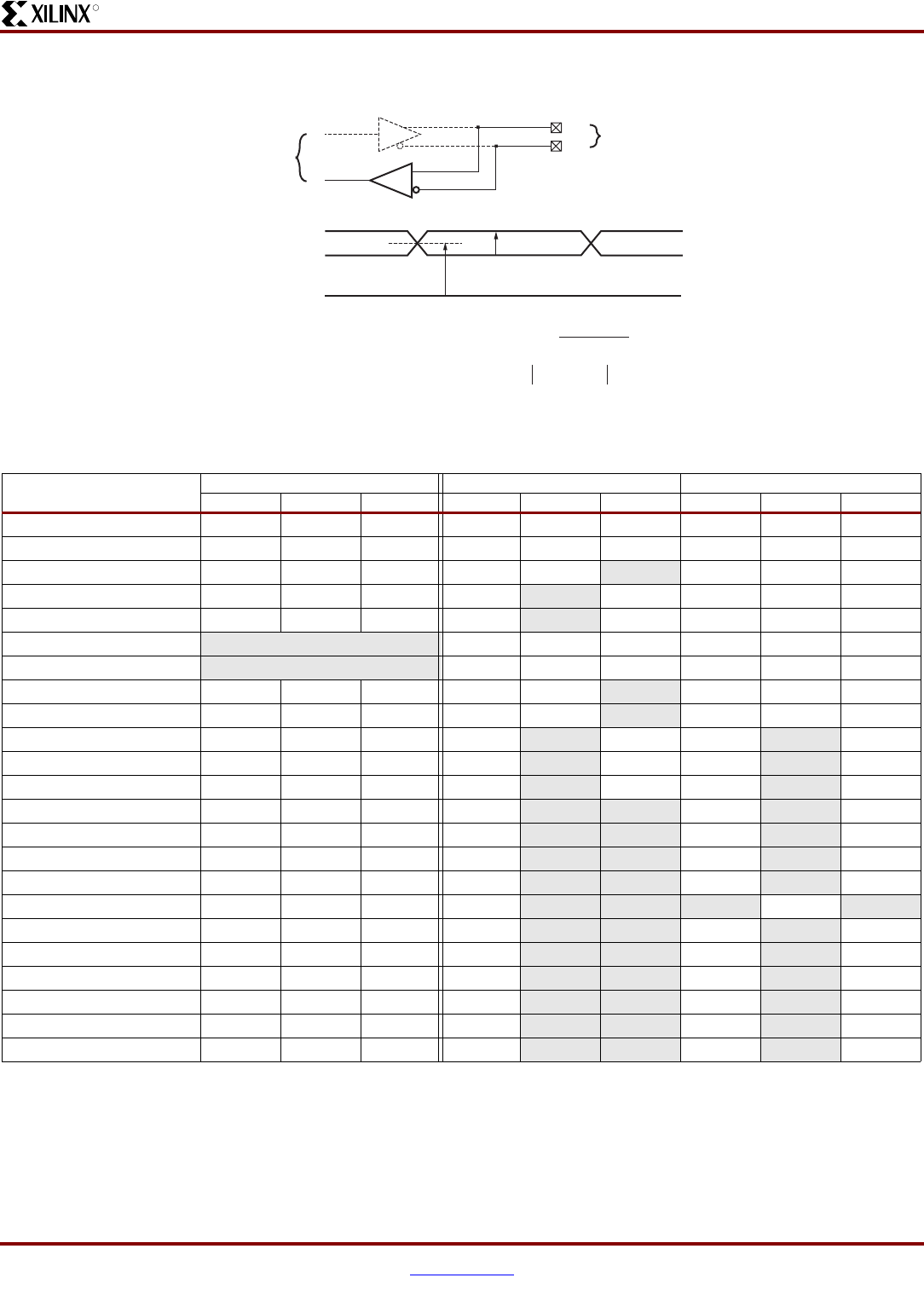
Figure 3:
Differential Input Voltages
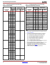
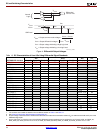
Table 12:
Recommended Operating Conditions for User I/Os Using Differential Signal Standards
IOSTANDARD Attribute
V
CCO
for Drivers
(1)
V
ID
V
ICM
(2)
Min (V) Nom (V) Max (V) Min (mV) Nom (mV) Max (mV) Min (V) Nom (V) Max (V)
LVDS_25
(3)
2.25 2.5 2.75 100 350 600 0.3 1.25 2.35
LVDS_33
(3)
3.0 3.3 3.6 100 350 600 0.3 1.25 2.35
BLVDS_25
(4)
2.25 2.5 2.75 100 300 – 0.3 1.3 2.35
MINI_LVDS_25
(3)
2.25 2.5 2.75 200 – 600 0.3 1.2 1.95
MINI_LVDS_33
(3)
3.0 3.3 3.6 200 – 600 0.3 1.2 1.95
LVPECL_25
(5)
Inputs Only 100 800 1000 0.3 1.2 1.95
LVPECL_33
(5)
Inputs Only 100 800 1000 0.3 1.2 2.8
(6)
RSDS_25
(3)
2.25 2.5 2.75 100 200 – 0.3 1.2 1.5
RSDS_33
(3)
3.0 3.3 3.6 100 200 – 0.3 1.2 1.5
TMDS_33
(3,4,7)
3.14 3.3 3.47 150 – 1200 2.7 –3.23
PPDS_25
(3)
2.25 2.5 2.75 100 –4000.2–2.3
PPDS_33
(3)
3.0 3.3 3.6 100 –4000.2–2.3
DIFF_HSTL_I_18
1.7 1.8 1.9 100
– –0.8–1.1
DIFF_HSTL_II_18
(8)
1.7 1.8 1.9 100 – –0.8–1.1
DIFF_HSTL_III_18
1.7 1.8 1.9 100
– –0.8–1.1
DIFF_HSTL_I
1.4 1.5 1.6 100
– –0.68–0.9
DIFF_HSTL_III
1.4 1.5 1.6 100
– – –0.9–
DIFF_SSTL18_I
1.7 1.8 1.9 100
– –0.7–1.1
DIFF_SSTL18_II
(8)
1.7 1.8 1.9 100 – –0.7–1.1
DIFF_SSTL2_I
2.3 2.5 2.7 100
– –1.0–1.5
DIFF_SSTL2_II
(8)
2.3 2.5 2.7 100 – –1.0–1.5
DIFF_SSTL3_I
3.0 3.3 3.6 100
– –1.1–1.9
DIFF_SSTL3_II
3.0 3.3 3.6 100
– –1.1–1.9
Notes:
1. The V
CCO
rails supply only differential output drivers, not input circuits.
2. V
ICM
must be less than V
CCAUX
.
3. These true differential output standards are supported only on FPGA banks 0 and 2. Inputs are unrestricted. See the chapter "Using I/O Resources" in UG331.
4. See "External Termination Requirements for Differential I/O."
5. LVPECL is supported on inputs only, not outputs. Requires V
CCAUX
=3.3V ± 10%.
6. LVPECL_33 maximum V
ICM
= V
CCAUX
– (V
ID
/2).
7. Requires V
CCAUX
= 3.3V ± 10%. (V
CCAUX
- 300 mV) ≤V
ICM
≤ (V
ICM
- 37 mV).
8. These higher-drive output standards are supported only on FPGA banks 1 and 3. Inputs are unrestricted. See the chapter "Using I/O Resources" in UG331.
9. V
REF
inputs are used for the DIFF_SSTL and DIFF_HSTL standards. The V
REF
settings are the same as for the single-ended versions in Table 11. Other differential
standards do not use V
REF
.
DS610-3_03_061507
V
INN
V
INN
V
INP
V
INP
GND level
50%
V
ICM
V
ICM
= Input common mode voltage =
V
ID
Internal
Logic
Differential
I/O Pair Pins
N
P
2
V
INP
+
V
INN
V
ID
= Differential input voltage =
V
INP
-
V
INN