


DC and Switching Characteristics
30 www.xilinx.com DS610-3 (v2.0) July 16, 2007
Product Specification
R
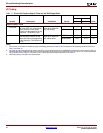
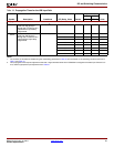
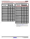
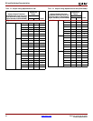
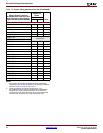
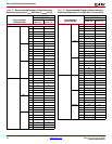
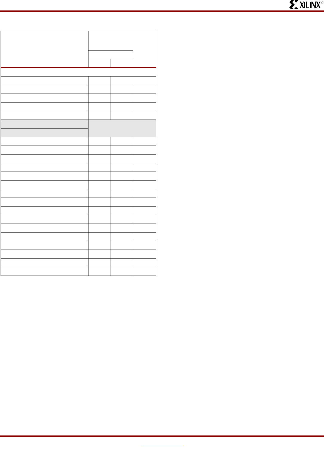
Differential Standards
LVDS_25 1.16 1.16 ns
LVDS_33 0.46 0.46 ns
BLVDS_25 0.11 0.11 ns
MINI_LVDS_25 0.75 0.75 ns
MINI_LVDS_33 0.40 0.40 ns
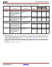
LVPECL_25
Inputs Only
LVPECL_33
RSDS_25 1.42 1.42 ns
RSDS_33 0.58 0.58 ns
TMDS_33 0.46 0.46 ns
PPDS_25 1.07 1.07 ns
PPDS_33 0.63 0.63 ns
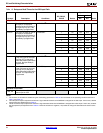
DIFF_HSTL_I_18 0.43 0.43 ns
DIFF_HSTL_II_18 0.41 0.41 ns
DIFF_HSTL_III_18 0.36 0.36 ns
DIFF_HSTL_I 1.01 1.01 ns
DIFF_HSTL_III 0.54 0.54 ns
DIFF_SSTL18_I 0.49 0.49 ns
DIFF_SSTL18_II 0.41 0.41 ns
DIFF_SSTL2_I 0.82 0.82 ns
DIFF_SSTL2_II 0.09 0.09 ns
DIFF_SSTL3_I 1.16 1.16 ns
DIFF_SSTL3_II 0.28 0.28 ns
Notes:
1. The numbers in this table are tested using the methodology
presented in Table 25 and are based on the operating conditions
set forth in Table 7, Table 10, and Table 12.
2. These adjustments are used to convert output- and
three-state-path times originally specified for the LVCMOS25
standard with 12 mA drive and Fast slew rate to times that
correspond to other signal standards. Do not adjust times that
measure when outputs go into a high-impedance state.
Table 24:
Output Timing Adjustments for IOB
(Continued)
Convert Output Time from
LVCMOS25 with 12mA Drive and
Fast Slew Rate to the Following
Signal Standard (IOSTANDARD)
Add the
Adjustment
Below
Units
Speed Grade
-5 -4