


DS610-1 (v2.0) July 16, 2007 www.xilinx.com 3
Product Specification
© 2007 Xilinx, Inc. All rights reserved. All Xilinx trademarks, registered trademarks, patents, and disclaimers are as listed at http://www.xilinx.com/legal.htm.
All other trademarks are the property of their respective owners. All specifications are subject to change without notice.
Introduction
The Spartan™-3A DSP family of Field-Programmable Gate Arrays
(FPGAs) solves the design challenges in most high-volume,
cost-sensitive, high-performance DSP applications.
The
two-member family offers densities ranging from
1.8 to 3.4
million
system gates, as shown in Table 1.
The Spartan-3A DSP family builds on the success of the
Spartan-3A FPGA family by increasing the amount of memory per
logic and adding XtremeDSP™ DSP48A slices. New features
improve system performance and reduce the cost of configuration.
These Spartan-3A DSP FPGA enhancements, combined with
proven 90 nm process technology, deliver more functionality and
bandwidth per dollar than ever before, setting the new standard in
the programmable logic
and DSP processing
industry.
Spartan-3A and Spartan-3A DSP FPGA Differences
The Spartan-3A DSP FPGAs extend and enhance the Spartan-3A
FPGA family. The XC3SD1800A and the XC3SD3400A devices
are tailored for DSP applications and have additional block RAM
and XtremeDSP DSP48A slices. The XtremeDSP DSP48A slices
replace the 18x18 multipliers found in the Spartan-3A devices and
are based on the DSP48 blocks found in the Virtex™-4 devices.
The block RAMs are also enhanced to run faster by adding an
output register. Both the block RAM and DSP48A slices in the
Spartan-3A DSP devices run at 250 MHz in the lowest cost,
standard -4 speed grade.
Because of their exceptional DSP price/performance ratio,
Spartan-3A DSP FPGAs are ideally suited to a wide range of
consumer electronics applications, including broadband access,
home networking, display/projection, and digital television
equipment.
The Spartan-3A DSP family is a superior alternative to mask
programmed ASICs. FPGAs avoid the high initial cost, lengthy
development cycles, and the inherent inflexibility of conventional
ASICs. Also, FPGA programmability permits design upgrades in
the field with no hardware replacement necessary, an impossibility
with ASICs.
Features
• Very low cost, high-performance DSP solution for
high-volume, cost-conscious applications
• 250 MHz XtremeDSP DSP48A Slices
♦
Dedicated 18-bit by 18-bit multiplier
♦ Available pipeline stages for enhanced performance of at least
250 MHz in the standard -4 speed grade
♦ 48-bit accumulator for multiply-accumulate (MAC) operation
♦ Integration added for complex multiply or multiply-add operation
♦ Integrated 18-bit pre-adder
♦ Optional cascaded Multiply or MAC
• Hierarchical SelectRAM™ memory architecture
♦
Up to 2268 Kbits of fast block RAM with byte write enables for
processor applications
♦ Up to 373 Kbits of efficient distributed RAM
♦ Registered outputs on the block RAM with operation of at least
280 MHz in the standard -4 speed grade
• Dual-range V
CCAUX
supply simplifies 3.3V-only design
• Suspend, Hibernate modes reduce system power
• Low-power option reduces quiescent current
• Multi-voltage, multi-standard SelectIO™ interface pins
♦
Up to 519 I/O pins or 227 differential signal pairs
♦ LVCMOS, LVTTL, HSTL, and SSTL single-ended I/O
♦ 3.3V, 2.5V, 1.8V, 1.5V, and 1.2V signaling
♦ Selectable output drive, up to 24 mA per pin
♦ QUIETIO standard reduces I/O switching noise
♦ Full 3.3V ± 10% compatibility and hot swap compliance
♦ 622+ Mb/s data transfer rate per differential I/O
♦ LVDS, RSDS, mini-LVDS, HSTL/SSTL differential I/O with
integrated differential termination resistors
♦ Enhanced Double Data Rate (DDR) support
♦ DDR/DDR2 SDRAM support up to 333 Mb/s
♦ Fully compliant 32-/64-bit, 33/66 MHz PCI support
• Abundant, flexible logic resources
♦
Densities up to 53712 logic cells, including optional shift register
♦ Efficient wide multiplexers, wide logic
♦ Fast look-ahead carry logic
♦ IEEE 1149.1/1532 JTAG programming/debug port
• Eight Digital Clock Managers (DCMs)
♦
Clock skew elimination (delay locked loop)
♦ Frequency synthesis, multiplication, division
♦ High-resolution phase shifting
♦ Wide frequency range (5 MHz to over 320 MHz)
• Eight low-skew global clock networks, eight additional clocks
per half device, plus abundant low-skew routing
• Configuration interface to industry-standard PROMs
♦
Low-cost, space-saving SPI serial Flash PROM
♦ x8 or x8/x16 parallel NOR Flash PROM
♦ Low-cost Xilinx Platform Flash with JTAG
♦ Unique Device DNA identifier for design authentication
♦ Load multiple bitstreams under FPGA control
• MicroBlaze™ and PicoBlaze™ embedded processor cores
• BGA and CSP packaging with Pb-free options
♦
Common footprints support easy density migration
<
B
L
B
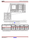
Spartan-3A DSP FPGA Family:
Introduction and Ordering Information
DS610-1 (v2.0) July 16, 2007 Product Specification
R
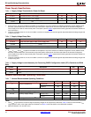
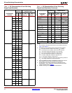
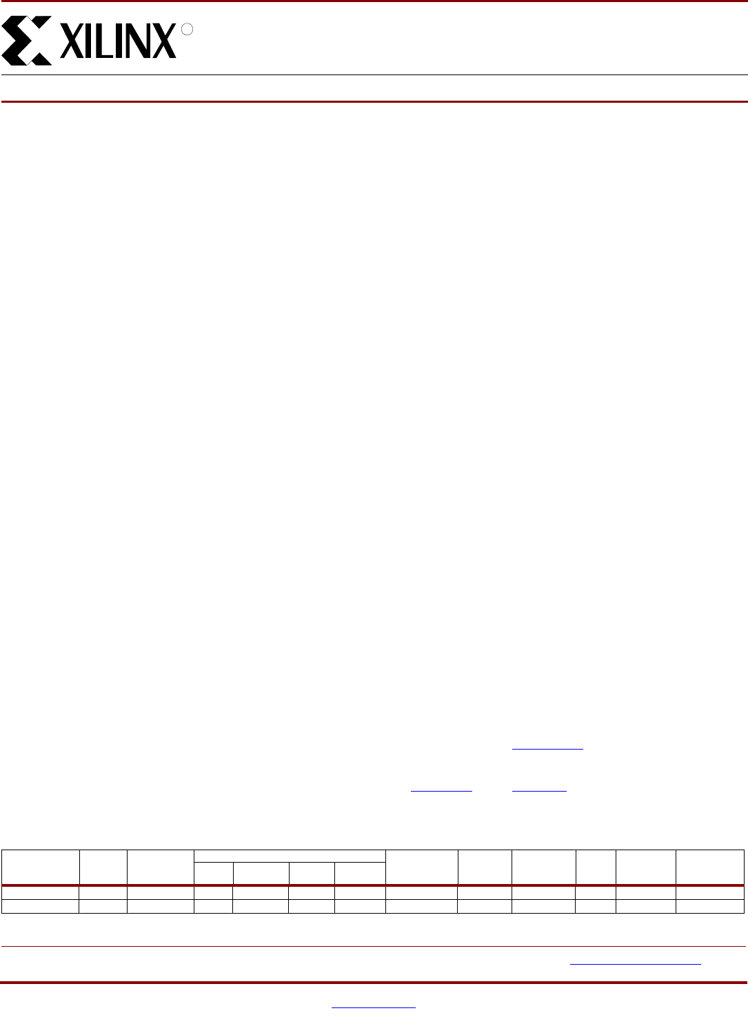
Table 1:
Summary of Spartan-3A DSP FPGA Attributes
Device
System
Gates
Equivalent
Logic Cells
CLB Array (One CLB = Four Slices)
Distributed
RAM
Bits
(1)
Block
RAM
Bits
(1)
DSP48As DCMs
Maximum
User I/O
Maximum
Differential
I/O PairsRows Columns
Total
CLBs
Total
Slices
XC3SD1800A 1800K 37,440 88 48 4160 16640 260K 1512K 84 8 519 227
XC3SD3400A 3400K 53,712 104 58 5968 23872 373K 2268K 126 8 469 213
Notes: 1. By convention, one Kb is equivalent to 1,024 bits.