


DC and Switching Characteristics
DS610-3 (v2.0) July 16, 2007 www.xilinx.com 37
Product Specification
R
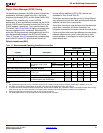
Clock Buffer/Multiplexer Switching Characteristics
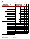
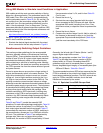
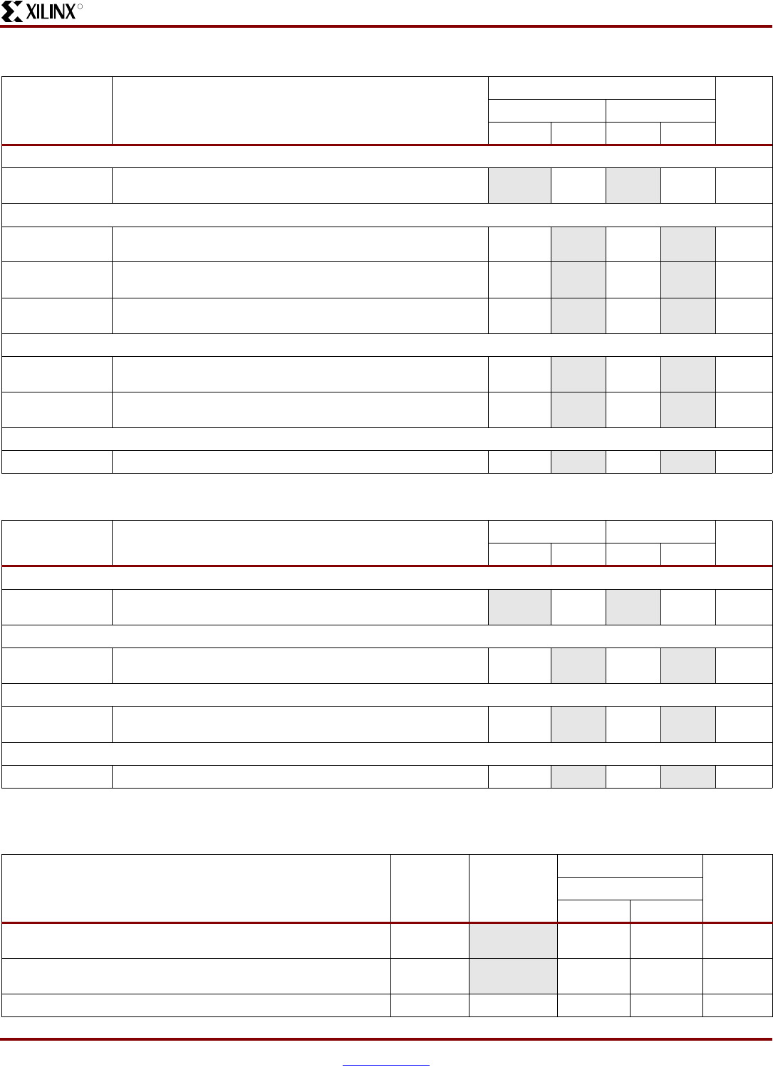
Table 29:
CLB Distributed RAM Switching Characteristics
Symbol Description
Speed Grade
Units
-5 -4
Min Max Min Max
Clock-to-Output Times
T
SHCKO
Time from the active edge at the CLK input to data appearing on
the distributed RAM output
-1.44-1.72ns
Setup Times
T
DS
Setup time of data at the BX or BY input before the active
transition at the CLK input of the distributed RAM
-0.07 --0.02-ns
T
AS
Setup time of the F/G address inputs before the active transition
at the CLK input of the distributed RAM
0.18 -0.36-ns
T
WS
Setup time of the write enable input before the active transition at
the CLK input of the distributed RAM
0.30 -0.59-ns
Hold Times
T
DH
Hold time of the BX and BY data inputs after the active transition
at the CLK input of the distributed RAM
0.13 -0.13-ns
T
AH,
T
WH
Hold time of the F/G address inputs or the write enable input after
the active transition at the CLK input of the distributed RAM
0.01 -0.01-ns
Clock Pulse Width
T
WPH
, T
WPL
Minimum High or Low pulse width at CLK input 0.88 -1.01-ns
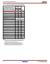
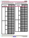
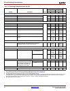
Table 30:
CLB Shift Register Switching Characteristics
Symbol Description
-5 -4
UnitsMin Max Min Max
Clock-to-Output Times
T
REG
Time from the active edge at the CLK input to data appearing on
the shift register output
-4.11-4.82ns
Setup Times
T
SRLDS
Setup time of data at the BX or BY input before the active
transition at the CLK input of the shift register
0.13 -0.18-ns
Hold Times
T
SRLDH
Hold time of the BX or BY data input after the active transition at
the CLK input of the shift register
0.16 -0.15-ns
Clock Pulse Width
T
WPH
, T
WPL
Minimum High or Low pulse width at CLK input 0.90 -1.01-ns
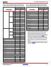
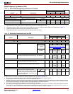
Table 31:
Clock Distribution Switching Characteristics
Description Symbol Minimum
Maximum
Units
Speed Grade
-5 -4
Global clock buffer (BUFG, BUFGMUX, BUFGCE) I input to
O-output delay
T
GIO
- 0.22 0.23 ns
Global clock multiplexer (BUFGMUX) select S-input setup to I0 and
I1 inputs. Same as BUFGCE enable CE-input
T
GSI
- 0.56 0.63 ns
Frequency of signals distributed on global buffers (all sides) F
BUFG
0350333MHz