


DC and Switching Characteristics
12 www.xilinx.com DS610-3 (v2.0) July 16, 2007
Product Specification
R
Power Supply Specifications
General Recommended Operating Conditions
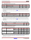
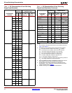
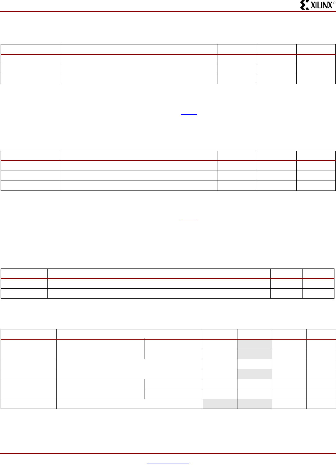
Table 4:
Supply Voltage Thresholds for Power-On Reset
Symbol Description Min Max Units
V
CCINTT
Threshold for the V
CCINT
supply 0.4 1.0 V
V
CCAUXT
Threshold for the V
CCAUX
supply 0.8 2.0 V
V
CCO2T
Threshold for the V
CCO
Bank 2 supply 0.8 2.0 V
Notes:
1. V
CCINT
, V
CCAUX
, and V
CCO
supplies to the FPGA can be applied in any order. However, the FPGA’s configuration source (Platform Flash,
SPI Flash, parallel NOR Flash, microcontroller) might have specific requirements. Check the data sheet for the attached configuration
source. Apply V
CCINT
last for lowest overall power consumption (see the UG331 chapter titled "Powering Spartan-3 Generation FPGAs" for
more information).
2. To ensure successful power-on, V
CCINT
, V
CCO
Bank 2, and V
CCAUX
supplies must rise through their respective threshold-voltage ranges with
no dips at any point.
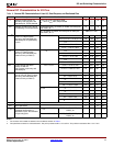
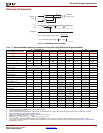
Table 5:
Supply Voltage Ramp Rate
Symbol Description Min Max Units
V
CCINTR
Ramp rate from GND to valid V
CCINT
supply level 0.2 100 ms
V
CCAUXR
Ramp rate from GND to valid V
CCAUX
supply level 0.2 100 ms
V
CCO2R
Ramp rate from GND to valid V
CCO
Bank 2 supply level 0.2 100 ms
Notes:
1. V
CCINT
, V
CCAUX
, and V
CCO
supplies to the FPGA can be applied in any order. However, the FPGA’s configuration source (Platform Flash,
SPI Flash, parallel NOR Flash, microcontroller) might have specific requirements. Check the data sheet for the attached configuration
source. Apply V
CCINT
last for lowest overall power consumption (see the UG331 chapter titled "Powering Spartan-3 Generation FPGAs" for
more information).
2. To ensure successful power-on, V
CCINT
, V
CCO
Bank 2, and V
CCAUX
supplies must rise through their respective threshold-voltage ranges with
no dips at any point.
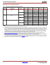
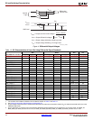
Table 6:
Supply Voltage Levels Necessary for Preserving CMOS Configuration Latch (CCL) Contents and RAM
Data
Symbol Description Min Units
V
DRINT
V
CCINT
level required to retain CMOS Configuration Latch (CCL) and RAM data 1.0 V
V
DRAUX
V
CCAUX
level required to retain CMOS Configuration Latch (CCL) and RAM data 2.0 V
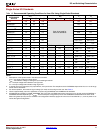
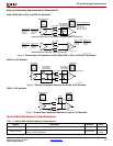
Table 7:
General Recommended Operating Conditions
Symbol Description Min Nominal Max Units
T
J
Junction temperature Commercial 0 -85°C
Industrial –40
-100°C
V
CCINT
Internal supply voltage 1.140 1.200 1.260 V
V
CCO
(1)
Output driver supply voltage 1.100 -3.600V
V
CCAUX
Auxiliary supply voltage V
CCAUX
= 2.5 2.250 2.500 2.750 V
V
CCAUX
= 3.3 3.000 3.300 3.600 V
T
IN
Input signal transition time
(2)
- - 500 ns
Notes:
1. This V
CCO
range spans the lowest and highest operating voltages for all supported I/O standards. Table 10 lists the recommended V
CCO
range specific to each of the single-ended I/O standards, and Table 12 lists that specific to the differential standards.
2. Measured between 10% and 90% V
CCO
.