


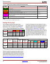
Pinout Descriptions
68 www.xilinx.com DS610-4 (v2.0) July 16, 2007
Product Specification
R
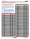
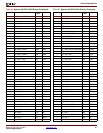
User I/Os by Bank
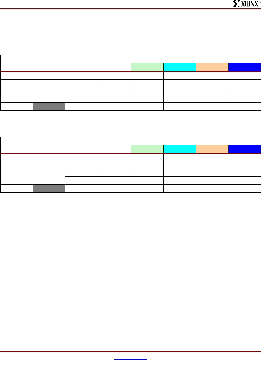
Table 61 and Tabl e 62 indicates how the user-I/O pins are
distributed between the four I/O banks on the CS484
package. The AWAKE pin is counted as a Dual-Purpose
I/O.
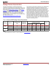
Footprint Migration Differences
There are no migration footprint differences between the
XC3SD1800A and the XC3SD3400A in the CS484
package.
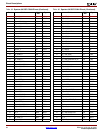
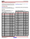
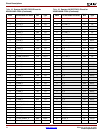
Table 61:
User I/Os Per Bank for the XC3SD1800A in the CS484 Package
Package
Edge
I/O Bank
Maximum I/Os
and
Input-Only
All Possible I/O Pins by Type
I/O INPUT DUAL VREF
(1)
CLK
Top 0 77 49 13 1 6 8
Right 1 78 23 9 30 8 8
Bottom 2 76 33 6 21 8 8
Left 3 78 51 13 0 6 8
TOTAL 309 156 41 52 28 32
Notes:
1. 19 VREF are on INPUT pins.
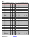
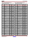
Table 62:
User I/Os Per Bank for the XC3SD3400A in the CS484 Package
Package
Edge
I/O Bank
Maximum I/O
and
Input-Only
All Possible I/O Pins by Type
I/O INPUT DUAL VREF
(1)
CLK
Top 0 77 49 13 1 6 8
Right 1 78 23 9 30 8 8
Bottom 2 76 33 6 21 8 8
Left 3 78 51 13 0 6 8
TOTAL 309 156 41 52 28 32
Notes:
1. 19 VREF are on INPUT pins.