


Pinout Descriptions
92 www.xilinx.com DS610-4 (v2.0) July 16, 2007
Product Specification
R
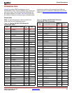
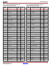
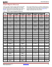
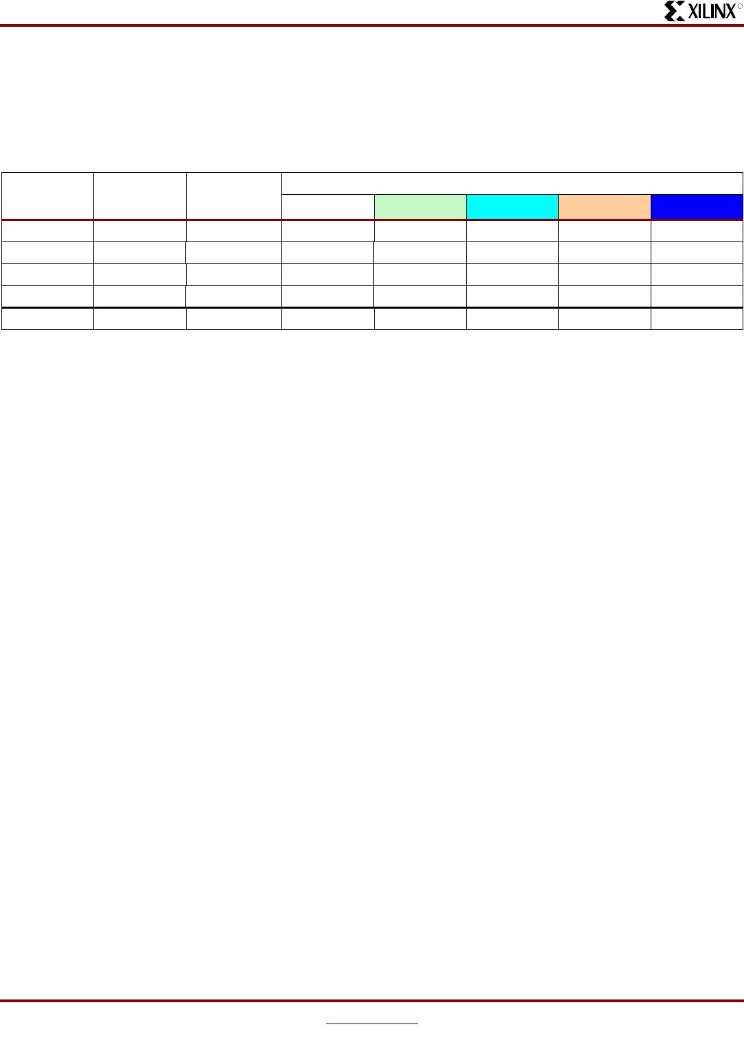
User I/Os by Bank
Table 66 indicates how the available user-I/O pins are
distributed between the four I/O banks on the FG676
package. The AWAKE pin is counted as a Dual-Purpose
I/O.
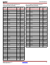
Table 66:
User I/Os Per Bank for the XC3SD3400A in the FG676 Package
Package
Edge
I/O Bank
Maximum I/Os
and
Input-Only
All Possible I/O Pins by Type
I/O INPUT DUAL VREF
(1)
CLK
Top 0 111 82 11 1 9 8
Right 1 123 67 8 30 10 8
Bottom 2 112 68 6 21 9 8
Left 3 123 97 9 0 9 8
TOTAL 46931434523732
Notes:
1. 26 VREF are on INPUT pins.