


DC and Switching Characteristics
DS610-3 (v2.0) July 16, 2007 www.xilinx.com 33
Product Specification
R
Using IBIS Models to Simulate Load Conditions in Application
IBIS models permit the most accurate prediction of timing
delays for a given application. The parameters found in the
IBIS model (V
REF
, R
REF
, and V
MEAS
) correspond directly
with the parameters used in Table 25 (V
T
, R
T
, and V
M
). Do
not confuse V
REF
(the termination voltage) from the IBIS
model with V
REF
(the input-switching threshold) from the
table. A fourth parameter, C
REF
, is always zero. The four
parameters describe all relevant output test conditions. IBIS
models are found in the Xilinx development software as well
as at the following link:
http://www.xilinx.com/xlnx/xil_sw_updates_home.jsp
Delays for a given application are simulated according to its
specific load conditions as follows:
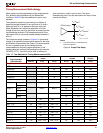
1. Simulate the desired signal standard with the output
driver connected to the test setup shown in Figure 8.
Use parameter values V
T
, R
T
, and V
M
from Ta bl e 25.
C
REF
is zero.
2. Record the time to V
M
.
3. Simulate the same signal standard with the output
driver connected to the PCB trace with load. Use the
appropriate IBIS model (including V
REF
, R
REF
, C
REF
,
and V
MEAS
values) or capacitive value to represent the
load.
4. Record the time to V
MEAS
.
5. Compare the results of steps 2 and 4. Add (or subtract)
the increase (or decrease) in delay to (or from) the
appropriate Output standard adjustment (Table 24) to
yield the worst-case delay of the PCB trace.
Simultaneously Switching Output Guidelines
This section provides guidelines for the recommended
maximum allowable number of Simultaneous Switching
Outputs (SSOs). These guidelines describe the maximum
number of user I/O pins of a given output signal standard
that should simultaneously switch in the same direction,
while maintaining a safe level of switching noise. Meeting
these guidelines for the stated test conditions ensures that
the FPGA operates free from the adverse effects of ground
and power bounce.
Ground or power bounce occurs when a large number of
outputs simultaneously switch in the same direction. The
output drive transistors all conduct current to a common
voltage rail. Low-to-High transitions conduct to the V
CCO
rail; High-to-Low transitions conduct to the GND rail. The
resulting cumulative current transient induces a voltage
difference across the inductance that exists between the die
pad and the power supply or ground return. The inductance
is associated with bonding wires, the package lead frame,
and any other signal routing inside the package. Other
variables contribute to SSO noise levels, including stray
inductance on the PCB as well as capacitive loading at
receivers. Any SSO-induced voltage consequently affects
internal switching noise margins and ultimately signal
quality.
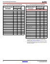
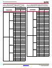
Table 26 and Ta ble 27 provide the essential SSO
guidelines. For each device/package combination, Table 26
provides the number of equivalent V
CCO
/GND pairs. For
each output signal standard and drive strength, Table 27
recommends the maximum number of SSOs, switching in
the same direction, allowed per V
CCO
/GND pair within an
I/O bank. The guidelines in Table 27 are categorized by
package style, slew rate, and output drive current.
Furthermore, the number of SSOs is specified by I/O bank.
Generally, the left and right I/O banks (Banks 1 and 3)
support higher output drive current.
Multiply the appropriate numbers from Table 26 and
Table 27 to calculate the maximum number of SSOs
allowed within an I/O bank. Exceeding these SSO
guidelines might result in increased power or ground
bounce, degraded signal integrity, or increased system jitter.
SSO
MAX
/IO Bank = Table 26 x Ta ble 27
The recommended maximum SSO values assumes that the
FPGA is soldered on the printed circuit board and that the
board uses sound design practices. The SSO values do not
apply for FPGAs mounted in sockets, due to the lead
inductance introduced by the socket.
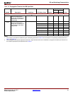
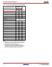
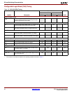
Table 26:
Equivalent V
CCO
/GND Pairs per Bank
Device
Package Style
(including Pb-free)
CS484 FG676
XC3SD1800A 6 9
XC3SD3400A 6 10