


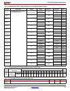
DC and Switching Characteristics
DS610-3 (v2.0) July 16, 2007 www.xilinx.com 45
Product Specification
R
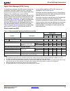
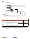
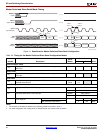
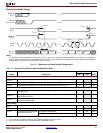
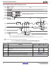
DNA Port Timing
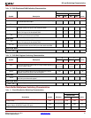
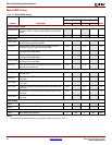
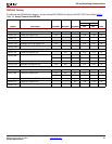
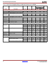
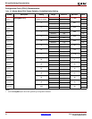
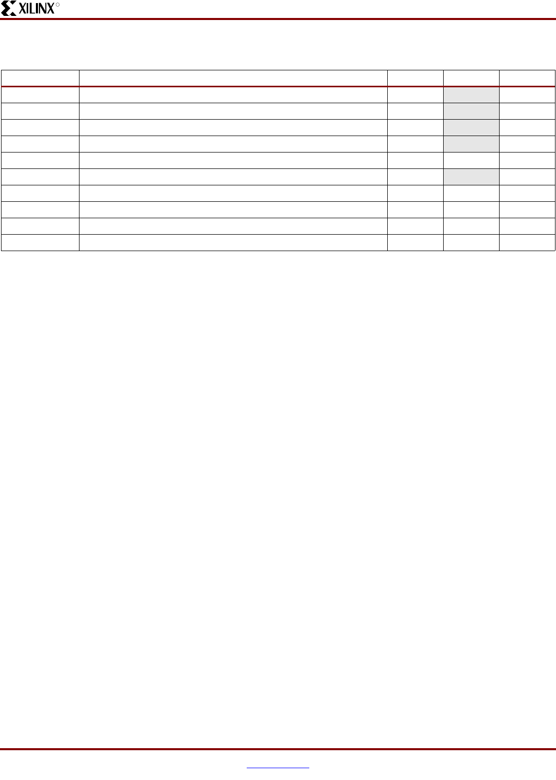
Table 42:
DNA_PORT Interface Timing
Symbol Description Min Max Units
T
DNASSU
Setup time on SHIFT before the rising edge of CLK 1.0 –ns
T
DNASH
Hold time on SHIFT after the rising edge of CLK 0.5 –ns
T
DNADSU
Setup time on DIN before the rising edge of CLK 1.0 –ns
T
DNADH
Hold time on DIN after the rising edge of CLK 0.5 –ns
T
DNARSU
Setup time on READ before the rising edge of CLK 5.0 10,000 ns
T
DNARH
Hold time on READ after the rising edge of CLK 0.0 –ns
T
DNADCKO
Clock-to-output delay on DOUT after rising edge of CLK 0.5 1.5 ns
T
DNACLKF
CLK frequency 0.0 100 MHz
T
DNACLKL
CLK High time 1.0 ∞ ns
T
DNACLKH
CLK Low time 1.0 ∞ ns
Notes:
1. The minimum READ pulse width is 5 ns, and the maximum READ pulse width is 10 μs.