


DC and Switching Characteristics
52 www.xilinx.com DS610-3 (v2.0) July 16, 2007
Product Specification
R
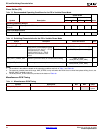
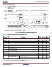
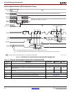
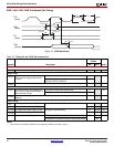
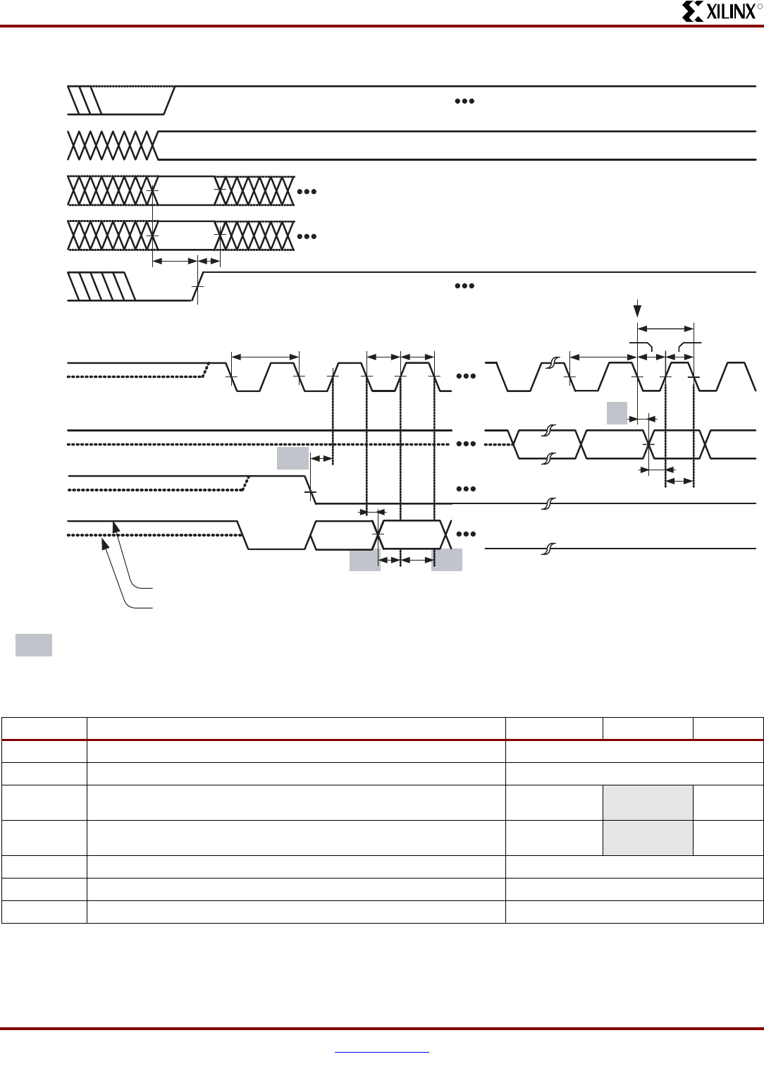
Serial Peripheral Interface (SPI) Configuration Timing
Figure 13:
Waveforms for Serial Peripheral Interface (SPI) Configuration
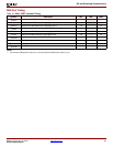
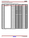
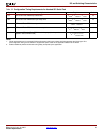
Table 51:
Timing for Serial Peripheral Interface (SPI) Configuration Mode
Symbol Description Minimum Maximum Units
T
CCLK1
Initial CCLK clock period (see Table 45)
T
CCLK
n
CCLK clock period after FPGA loads ConfigRate setting (see Table 45)
T
MINIT
Setup time on CSI_B, RDWR_B, and M[2:0] mode pins before the rising
edge of INIT_B
50 -ns
T
INITM
Hold time on CSI_B, RDWR_B, and M[2:0] mode pins after the rising edge
of INIT_B
0 -ns
T
CCO
Address A[25:0] outputs valid after CCLK falling edge See Table 49
T
DCC
Setup time on D[7:0] data inputs before CCLK falling edge See Table 49
T
CCD
Hold time on D[7:0] data inputs after CCLK falling edge See Table 49
T
DH
T
DSU
Command
(msb)
T
V
T
CSS
<1:1:1>
INIT_B
M[2:0]
T
MINIT
T
INITM
DIN
CCLK
(Input)
T
CCLKn
T
CCLK1
VS[2:0]
(Input)
New ConfigRate active
Mode input pins M[2:0] and variant select input pins VS[2:0] are sampled when INIT_B
goes High. After this point, input values do not matter until DONE goes High, at which
point these pins become user-I/O pins.
<0:0:1>
Pin initially pulled High by internal pull-up resistor if PUDC_B input is Low.
Pin initially high-impedance (Hi-Z) if PUDC_B input is High. External pull-up resistor required on CSO_B.
T
CCLK1
T
MCCLn
T
MCCHn
(Input)
Data Data Data Data
CSO_B
MOSI
T
CCO
T
MCCL1
T
MCCH1
T
DCC
T
CCD
(Input)
PROG_B
PUDC_B
(Input)
PUDC_B must be stable before INIT_B goes High and constant throughout the configuration process.
DS529-3_06_102506
(Open-Drain)
Shaded values indicate specifications on attached SPI Flash PROM.
Command
(msb-1)