


Introduction and Ordering Information
DS610-1 (v2.0) July 16, 2007 www.xilinx.com 5
Product Specification
R
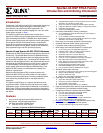
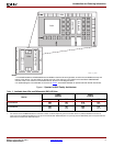
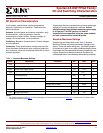
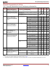
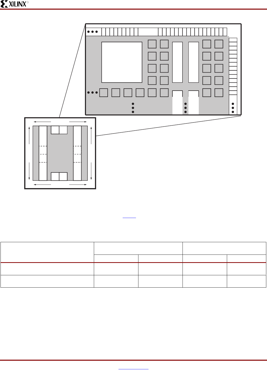
Figure 1:
Spartan-3A DSP Family Architecture
CLB
Block RAM
DCM
IOBs
IOBs
DS610-1_01_031207
IOBs
IOBs
DCM
Block RAM / DSP48A Slice
DCM
CLBs
IOBs
DSP48A Slice
Notes:
1. The XC3SD1800A and XC3SD3400A have two DCMs on both the left and right sides, as well as the two DCMs at the top and
bottom of the devices. The two DCMs on the left and right of the chips are in the middle of the outer Block RAM/DSP48A
columns of the 4 or 5 columns in the selected device, as shown in the diagram above.
2. A detailed diagram of the DSP48A can be found in U
G431:
XtremeDSP DSP48A for Spartan-3A DSP FPGAs User Guide.
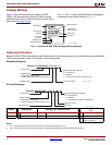
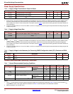
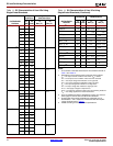
Table 2:
Available User I/Os and Differential (Diff) I/O Pairs
Device
CS484
CSG484
FG676
FGG676
User Diff User Diff
XC3SD1800A
309
(60)
140
(78)
519
(110)
227
(131)
XC3SD3400A
309
(60)
140
(78)
469
(60)
213
(117)
Notes:
1. The number shown in bold indicates the maximum number of I/O and input-only pins. The number shown in
(
italics
) indicates the number of
input-only pins. The differential (Diff) input-only pin count includes both differential pairs on input-only pins and differential pairs on I/O pins within I/O
banks that are restricted to differential inputs.