


Pinout Descriptions
DS610-4 (v2.0) July 16, 2007 www.xilinx.com 83
Product Specification
R
XC3SD3400A FPGA
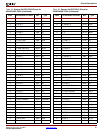
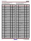
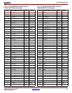
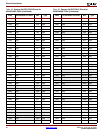
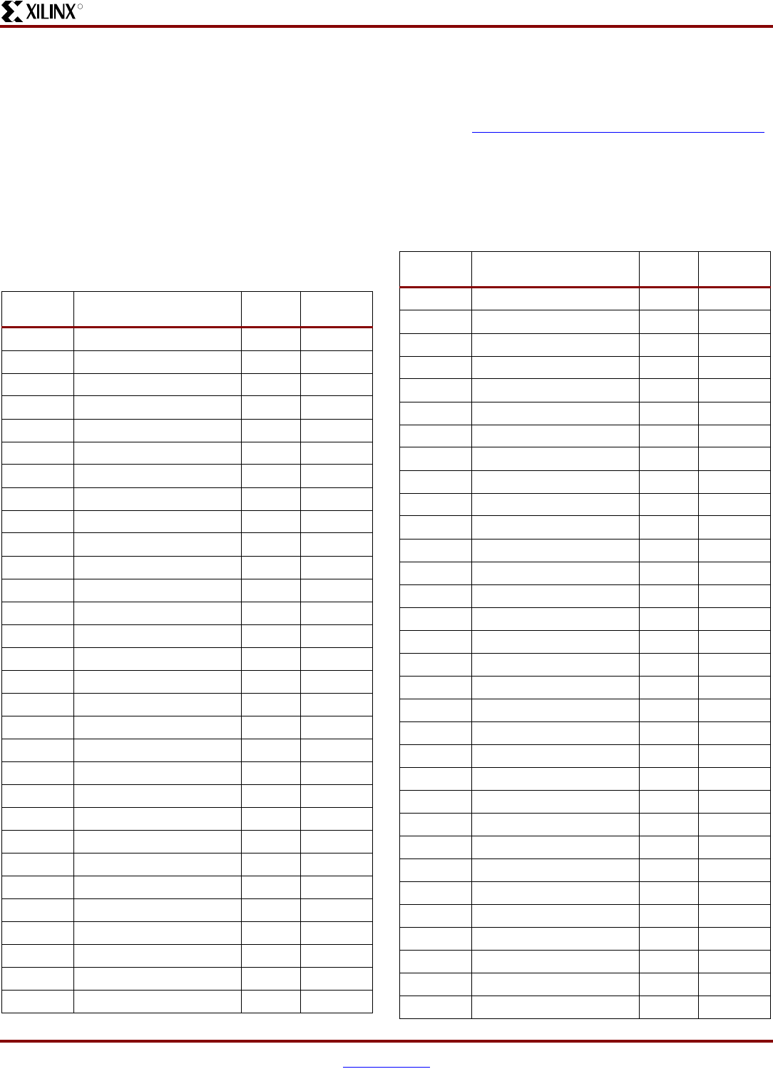
Table 65 lists all the FG676 package pins for the
XC3SD3400A FPGA. They are sorted by bank number and
then by pin name. Pairs of pins that form a differential I/O
pair appear together in the table. Table 65 also shows the
pin number for each pin and the pin type, as defined earlier.
An electronic version of this package pinout table and
footprint diagram is available for download from the Xilinx
website at:
http://www.xilinx.com/bvdocs/publications/s3adsp_pin.zip
Pinout Table
Note:
The grayed boxes denote a difference between the
XC3SD1800A and the XC3SD3400A devices.
Table 65:
Spartan-3A DSP FG676 Pinout for
XC3SD3400A FPGA
Bank XC3SD3400A Pin Name
FG676
Ball
Type
0 IO_L43N_0 K11 I/O
0 IO_L39N_0 K12 I/O
0 IO_L25P_0/GCLK4 K14 GCLK
0 IO_L12N_0 K16 I/O
0 IP_0 J10 INPUT
0 IO_L43P_0 J11 I/O
0 IO_L39P_0 J12 I/O
0 IP_0 J13 INPUT
0 IO_L25N_0/GCLK5 J14 GCLK
0 IP_0 J15 INPUT
0 IO_L12P_0 J16 I/O
0 IP_0/VREF_0 J17 VREF
0 IO_L47N_0 H9 I/O
0 IO_L46N_0 H10 I/O
0 IO_L35N_0 H12 I/O
0 IP_0 H13 INPUT
0 IO_L16N_0 H15 I/O
0 IO_L08P_0 H17 I/O
0 IP_0 H18 INPUT
0 IO_L52N_0/PUDC_B G8 DUAL
0 IO_L47P_0 G9 I/O
0 IO_L46P_0 G10 I/O
0 IP_0/VREF_0 G11 VREF
0 IO_L35P_0 G12 I/O
0 IO_L27N_0/GCLK9 G13 GCLK
0 IP_0 G14 INPUT
0 IO_L16P_0 G15 I/O
0 IO_L08N_0 G17 I/O
0 IO_L02P_0/VREF_0 G19 VREF
0 IO_L01P_0 G20 I/O
0 IO_L48P_0 F7 I/O
0 IO_L52P_0/VREF_0 F8 VREF
0 IO_L31N_0 F12 I/O
0 IO_L27P_0/GCLK8 F13 GCLK
0 IO_L24N_0 F14 I/O
0 IO_L20P_0 F15 I/O
0 IO_L13P_0 F17 I/O
0 IO_L02N_0 F19 I/O
0 IO_L01N_0 F20 I/O
0 IO_L48N_0 E7 I/O
0 IO_L37P_0 E10 I/O
0 IP_0 E11 INPUT
0 IO_L31P_0 E12 I/O
0 IO_L24P_0 E14 I/O
0 IO_L20N_0/VREF_0 E15 VREF
0 IO_L13N_0 E17 I/O
0 IP_0 E18 INPUT
0 IO_L10P_0 E21 I/O
0 IO_L44N_0 D6 I/O
0 IP_0/VREF_0 D7 VREF
0 IO_L40N_0 D8 I/O
0 IO_L37N_0 D9 I/O
0 IO_L34N_0 D10 I/O
0 IO_L32N_0/VREF_0 D11 VREF
0 IP_0 D12 INPUT
0 IO_L30P_0 D13 I/O
0 IP_0/VREF_0 D14 VREF
0 IO_L22P_0 D16 I/O
0 IO_L21P_0 D17 I/O
0 IO_L17P_0 D18 I/O
0 IO_L11P_0 D20 I/O
0 IO_L10N_0 D21 I/O
Table 65:
Spartan-3A DSP FG676 Pinout for
XC3SD3400A FPGA
(Continued)
Bank XC3SD3400A Pin Name
FG676
Ball
Type