


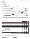
DC and Switching Characteristics
DS610-3 (v2.0) July 16, 2007 www.xilinx.com 55
Product Specification
R
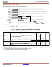
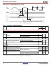
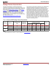
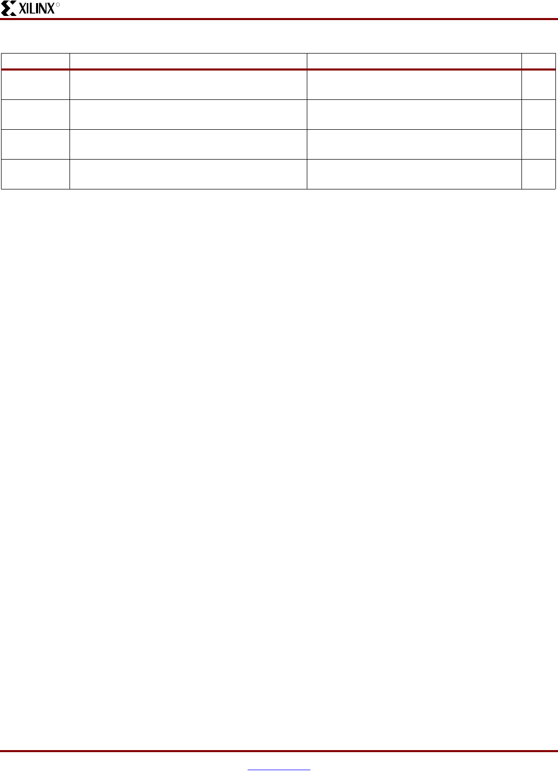
Table 54:
Configuration Timing Requirements for Attached Parallel NOR Flash
Symbol Description Requirement Units
T
CE
(t
ELQV
)
Parallel NOR Flash PROM chip-select time ns
T
OE
(t
GLQV
)
Parallel NOR Flash PROM output-enable time ns
T
ACC
(t
AVQV
)
Parallel NOR Flash PROM read access time ns
T
BYTE
(t
FLQV,
t
FHQV
)
For x8/x16 PROMs only: BYTE# to output valid time
(3)
ns
Notes:
1. These requirements are for successful FPGA configuration in BPI mode, where the FPGA generates the CCLK signal. The
post-configuration timing can be different to support the specific needs of the application loaded into the FPGA.
2. Subtract additional printed circuit board routing delay as required by the application.
3. The initial BYTE# timing can be extended using an external, appropriately sized pull-down resistor on the FPGA’s LDC2 pin. The resistor
value also depends on whether the FPGA’s PUDC_B pin is High or Low.
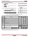
T
CE
T
INITADD
R
≤
T
OE
T
INITADD
R
≤
T
ACC
T
CCLKn min
()
T
CCO
T
DCC
PC
B
–––≤
T
BYTE
T
INITADD
R
≤