


DC and Switching Characteristics
42 www.xilinx.com DS610-3 (v2.0) July 16, 2007
Product Specification
R
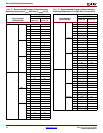
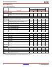
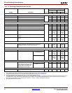
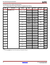
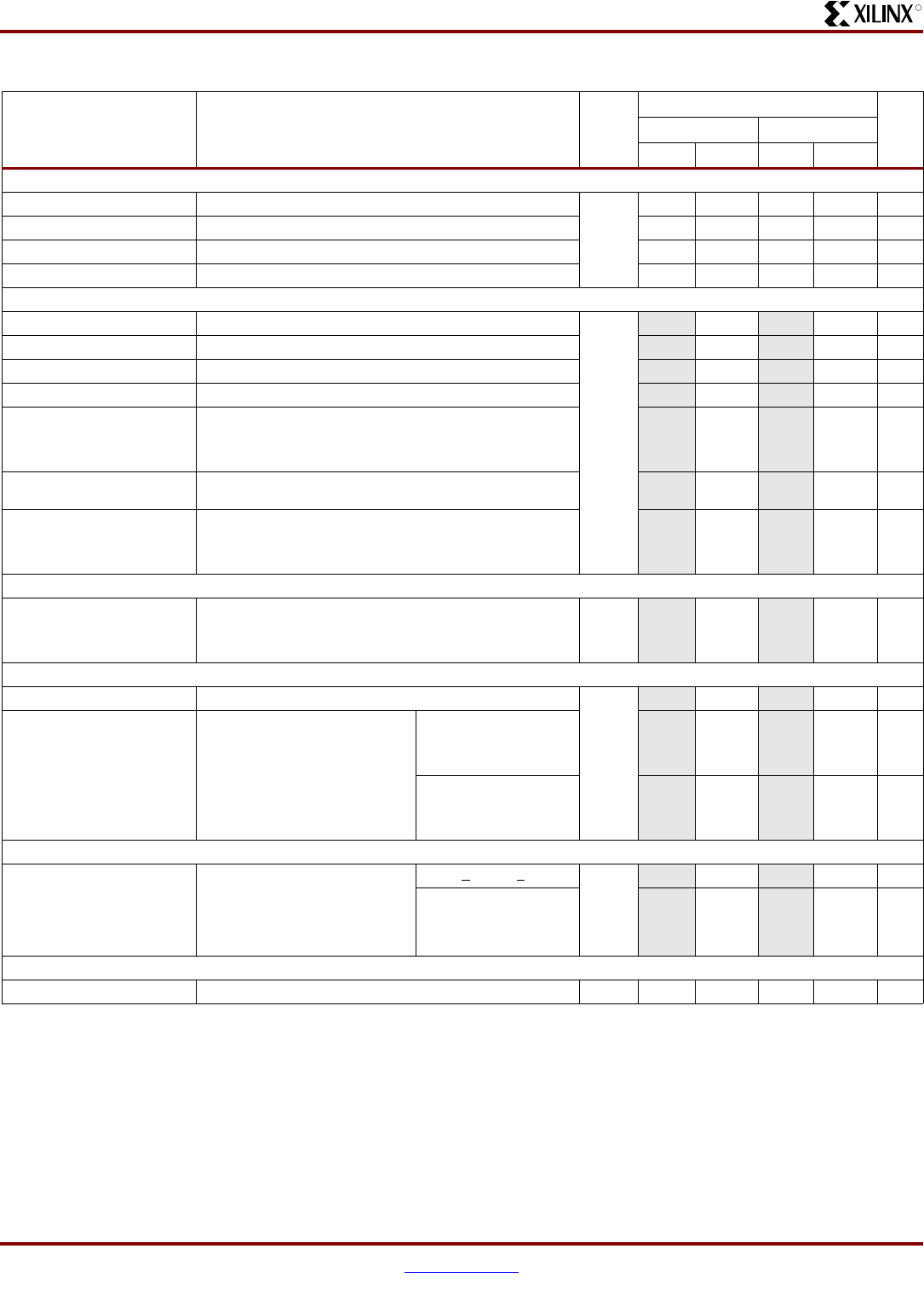
Table 36:
Switching Characteristics for the DLL
Symbol Description Device
Speed Grade
Units
-5 -4
Min Max Min Max
Output Frequency Ranges
CLKOUT_FREQ_CLK0 Frequency for the CLK0 and CLK180 outputs All 5 280 5 250 MHz
CLKOUT_FREQ_CLK90 Frequency for the CLK90 and CLK270 outputs 5 200 5 200 MHz
CLKOUT_FREQ_2X Frequency for the CLK2X and CLK2X180 outputs 10 334 10 334 MHz
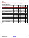
CLKOUT_FREQ_DV Frequency for the CLKDV output 0.3125 186 0.3125 166 MHz
Output Clock Jitter
(2,3,4)
CLKOUT_PER_JITT_0 Period jitter at the CLK0 output All - ±100 - ±100 ps
CLKOUT_PER_JITT_90 Period jitter at the CLK90 output
- ±150 - ±150 ps
CLKOUT_PER_JITT_180 Period jitter at the CLK180 output
- ±150 - ±150 ps
CLKOUT_PER_JITT_270 Period jitter at the CLK270 output
- ±150 - ±150 ps
CLKOUT_PER_JITT_2X Period jitter at the CLK2X and CLK2X180 outputs
- ±[0.5%
of CLKIN
period
+ 100]
- ±[0.5%
of CLKIN
period
+ 100]
ps
CLKOUT_PER_JITT_DV1 Period jitter at the CLKDV output when performing integer
division
- ±150 - ±150 ps
CLKOUT_PER_JITT_DV2 Period jitter at the CLKDV output when performing non-integer
division
- ±[0.5%
of CLKIN
period
+ 100]
- ±[0.5%
of CLKIN
period
+ 100]
ps
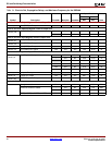
Duty Cycle
(4)
CLKOUT_DUTY_CYCLE_DLL Duty cycle variation for the CLK0, CLK90, CLK180, CLK270,
CLK2X, CLK2X180, and CLKDV outputs, including the
BUFGMUX and clock tree duty-cycle distortion
All
-±[1% of
CLKIN
period
+ 350]
-±[1% of
CLKIN
period
+ 350]
ps
Phase Alignment
(4)
CLKIN_CLKFB_PHASE Phase offset between the CLKIN and CLKFB inputs All - ±150 - ±150 ps
CLKOUT_PHASE_DLL Phase offset between DLL outputs
CLK0 to CLK2X
(not CLK2X180)
-±[1% of
CLKIN
period
+ 100]
-±[1% of
CLKIN
period
+ 100]
ps
All others
-±[1% of
CLKIN
period
+ 150]
-±[1% of
CLKIN
period
+ 150]
ps
Lock Time
LOCK_DLL
(3)
When using the DLL alone: The
time from deassertion at the DCM’s
Reset input to the rising transition
at its LOCKED output. When the
DCM is locked, the CLKIN and
CLKFB signals are in phase
5 MHz <
F
CLKIN
< 15 MHz All -5-5ms
F
CLKIN
> 15 MHz - 600 - 600 μs
Delay Lines
DCM_DELAY_STEP
(5)
Finest delay resolution, averaged over all steps All 15 35 15 35 ps
Notes:
1. The numbers in this table are based on the operating conditions set forth in Table 7 and Table 35.
2. Indicates the maximum amount of output jitter that the DCM adds to the jitter on the CLKIN input.
3. For optimal jitter tolerance and faster lock time, use the CLKIN_PERIOD attribute.
4. Some jitter and duty-cycle specifications include 1% of input clock period or 0.01 UI. For example, the data sheet specifies a maximum jitter of “±[1%
of CLKIN period + 150]”. Assume the CLKIN frequency is 100 MHz. The equivalent CLKIN period is 10 ns and 1% of 10 ns is 0.1 ns or 100 ps.
According to the data sheet, the maximum jitter is ±[100 ps + 150 ps] = ±250 ps
, averaged over all steps.
5. The typical delay step size is 23 ps.