


DC and Switching Characteristics
DS610-3 (v2.0) July 16, 2007 www.xilinx.com 53
Product Specification
R
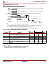
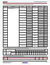
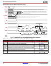
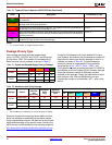
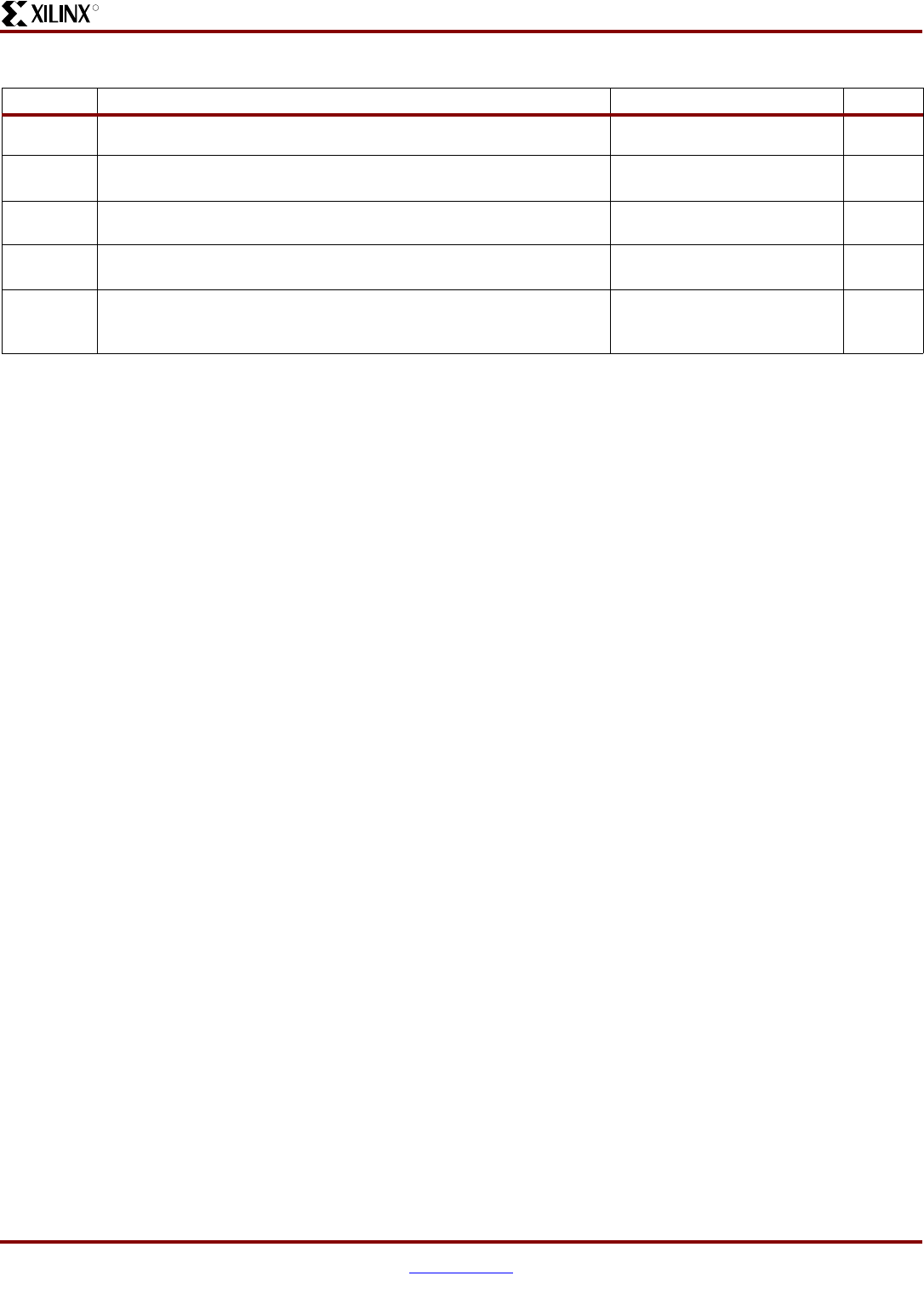
Table 52:
Configuration Timing Requirements for Attached SPI Serial Flash
Symbol Description Requirement Units
T
CCS
SPI serial Flash PROM chip-select time ns
T
DSU
SPI serial Flash PROM data input setup time ns
T
DH
SPI serial Flash PROM data input hold time ns
T
V
SPI serial Flash PROM data clock-to-output time ns
f
C
or f
R
Maximum SPI serial Flash PROM clock frequency (also depends on
specific read command used)
MHz
Notes:
1. These requirements are for successful FPGA configuration in SPI mode, where the FPGA generates the CCLK signal. The
post-configuration timing can be different to support the specific needs of the application loaded into the FPGA.
2. Subtract additional printed circuit board routing delay as required by the application.
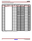
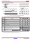
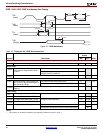
T
CCS
T
MCCL
1
T
CCO
–≤
T
DSU
T
MCCL
1
T
CCO
–≤
T
DH
T
MCCH
1
≤
T
V
T
MCCLn
T
DCC
–≤
f
C
1
T
CCLKn min
()
---------------------------------≥