


324 Instruction Latencies Appendix C
25112 Rev. 3.06 September 2005
Software Optimization Guide for AMD64 Processors
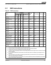
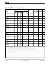
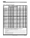
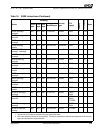
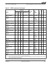
SHUFPS xmmreg1,
xmmreg2, imm8
0Fh C6h 11-xxx-xxx VectorPath FMUL 4 1
SHUFPS xmmreg,
mem128, imm8
0Fh C6h mm-xxx-xxx VectorPath FMUL 6 2
SQRTPS xmmreg1,
xmmreg2
0Fh 51h 11-xxx-xxx Double FMUL 39
SQRTPS xmmreg,
mem128
0Fh 51h mm-xxx-xxx Double FMUL 41
SQRTSS xmmreg1,
xmmreg2
F3h 0Fh 51h 11-xxx-xxx DirectPath FMUL 19
SQRTSS xmmreg,
mem32
F3h 0Fh 51h mm-xxx-xxx DirectPath FMUL 21
STMXCSR mem32 0Fh AEh mm-011-xxx VectorPath 11 4
SUBPS xmmreg1,
xmmreg2
0Fh 5Ch 11-xxx-xxx Double FADD 5 1
SUBPS xmmreg,
mem128
0Fh 5Ch mm-xxx-xxx Double FADD 7 1
SUBSS xmmreg1,
xmmreg2
F3h 0Fh 5Ch 11-xxx-xxx DirectPath FADD 4
SUBSS xmmreg,
mem32
F3h 0Fh 5Ch mm-xxx-xxx DirectPath FADD 6
UCOMISS xmmreg1,
xmmreg2
0Fh 2Eh 11-xxx-xxx VectorPath 4
UCOMISS xmmreg,
mem32
0Fh 2Eh mm-xxx-xxx VectorPath 6
UNPCKHPS xmmreg1,
xmmreg2
0Fh 15h 11-xxx-xxx Double FMUL 3 1
UNPCKHPS xmmreg,
mem128
0Fh 15h mm-xxx-xxx Double FMUL 5 1
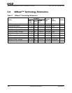
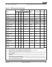
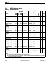
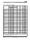
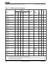
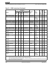
Table 18. SSE Instructions (Continued)
Syntax
Encoding
Decode
type
FPU pipe(s) Latency Note
Prefix
byte
First
byte
2nd
byte
ModRM byte
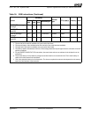
Notes:
1. The low half of the result is available one cycle earlier than listed.
2. The second latency value indicates when the low half of the result becomes available.
3. The high half of the result is available one cycle earlier than listed.
4. The latency listed is the absolute minimum, while average latencies may be higher and are a function of internal
pipeline conditions.
5. For the PREFETCHNTA/T0/T1/T2 instructions, the mem8 value refers to an address in the 64-byte line to be
prefetched.
6. The 8-clock latency is only visible to younger stores that need to do an external write. The 2-clock latency is
visible to the other stores and instructions.
7. This is the execution latency for the instruction. The time to complete the external write depends on the memory
speed and the hardware implementation.