346 AGP Considerations Appendix D
25112 Rev. 3.06 September 2005
Software Optimization Guide for AMD64 Processors
The theoretical data bandwidths for fast writes at 2x, 4x, and 8x are approximately 528 Mbytes/s,
1.056 Gbytes/s, and 2.1 Gbytes/s, respectively. These numbers are theoretical in terms of sustained
bursts occurring on the AGP bus. In actuality, data bandwidth depends on the size of the data block
transferred from the processor—larger block transfers are better.
Real bandwidth will be lower than the theoretical bandwidth because the beginning of fast-write
transactions require sending a PCI-protocol start transaction cycle (for the address phase) at the 1x
transfer rate instead of the higher speeds (2x, 4x, or 8x).
Larger block transfers help hide the transaction-start overhead (smaller block transfers have lower
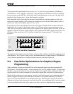
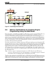
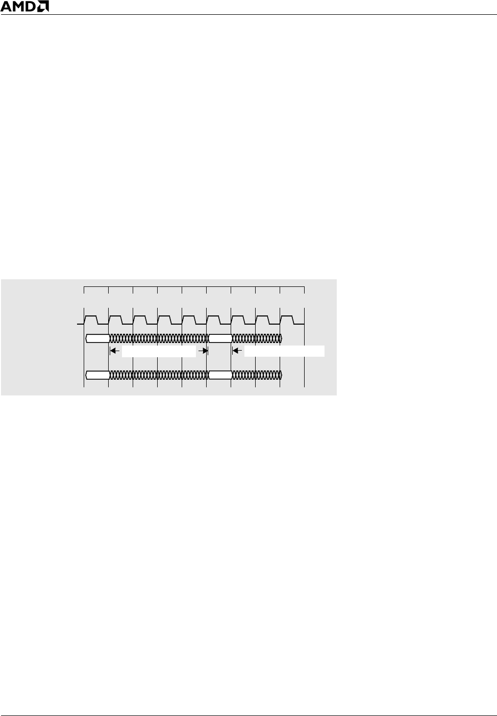
bandwidth). For example, at the 8x data-transfer rate, 128 bytes of data can be transferred in four
AGP clock cycles, but one initial clock cycle is required for the address phase. Five clock cycles are
required to transfer 128 bytes of data; therefore, the overhead of the address phase (clock cycle 1) for
128 bytes of data transferred is 20% (yielding a bandwidth of approximately 1.7 Gbytes/s). See
Figure 10.
Figure 10. AGP 8x Fast-Write Transaction
The overhead of the address phase for 64 bytes of data is 33% (yielding a bandwidth of approximately
1400 Mbytes/s). For 32 bytes of data (or less), the bandwidth drops to approximately 1000 Mbytes/s.
A key software optimization is to buffer as much processor write data as practical.
D.2 Fast-Write Optimizations for Graphics-Engine
Programming
Write-combining provides excellent AGP fast-write bandwidth when using the programmed I/O
(PIO) model—not the DMA model—for programming 2-D and 3-D graphics engines. To help ensure
that data is sent in optimal block sizes, you can “shadow” the engine’s render commands (that is, the
registers needed for a render command) in cache-block-aligned data structures in system memory.
Shadowing the structure in system memory (instead of writing the actual write-combining buffer in
memory-mapped I/O space) ensures that the write buffer is not emptied prematurely by external
events (such as an uncacheable read or hardware interrupt). Shadowing also ensures that writes to
different cache lines in the structure do not flush (close) the write-combining buffer since the number
of write-combining buffers that can be open at one time is processor-implementation dependent.
CLK
AD
C/BE
1
23456789
CMD
ADD
First block (128 bytes)
Second block (64 bytes)
ADD
CMD


