


Operation of Control Parts
CL-S6621 2-38
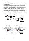
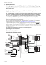
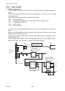
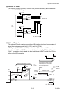
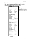
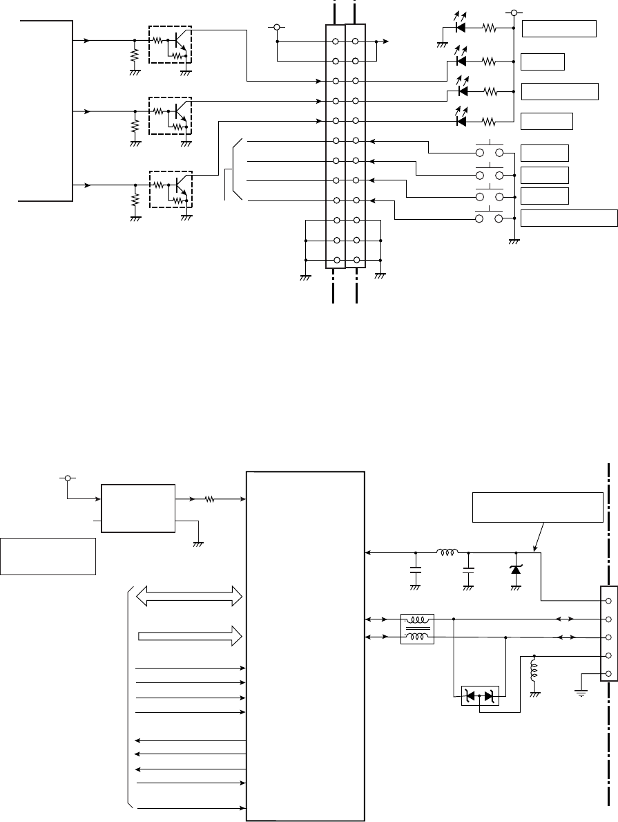
(4) Ope-pane circuit
The ope-pane circuit consists of 4 LEDs and 4 switches.
U14 (FPGA) controls the transistors (Q2 to Q4) to turn ON/OFF the LEDs. Each switch signal
is input to U1A (CPU). (The following shows the simplified circuit diagram.)
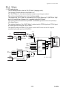
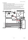
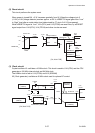
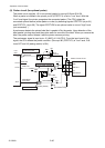
(5) USB I/F control circuit
The USB I/F control circuit supports the interface with a high-speed USB2.0 device.
It consists of U28 (high-speed USB2.0 controller) and peripheral circuits.
X3 (clock generator) generates a 48MHz clock for U28. Pins 41 (VBUS), 39 (DM0) and 40
(DP0) are for USB interface. U28 is controlled by U1A (CPU).
3
4
1
4
5
2
J4
6
7
8
+3.3V
[SA, Main PCB]
9
10
11
12
PRTLED
CNDLED
ERRLED
SW/STOP
SW/MODE
SW/PAUSE
SW/FEED
+3.3V
[SA, Opepane PCB]
POWER ON (Green)
PRINT (Green)
CONDITION (Orange)
ERROR (Red)
FEED
PAUSE
STOP
MODE/REPEAT
+3.3V
D304
D303
D302
SW302
SW303
SW304
SW301
D301
3
4
1
4
5
2
CN301
6
7
8
9
10
11
12
To
U1A CPU
B1_9
U14
FPGA
Q4
DTC114EM
LED_R
R142
E1
Q3
DTC114EM
LED_O
R141
Q2
DTC114EM
LED_G
R140
B3_31
L16
B3_30
L15
1
2
3
4
5
D7
L7
J18
L8
C137
L6
SG
USBVCC
USBLGND
DP
DM
USB I/F
[SA, Main PCB]
C138
D6
RD_N
WR0_N
WR1_N
CS_N
U28
R8A66597FP
To/From
U1A CPU
D0-D15
A1-A7
High Speed USB2.0 Controller
SOF_N
DREQ0_N
RST_N
DACK0_N
62-69
72-79
47-49
52-55
D0-D15
A1-A7
INT_N
G
+3.3V
Clock Generator
Clock for USB2.0
(48MHz)
X3
V
SB
C
23
4
1
3
2
R129
DSC8002DI1
(48MHz)
XIN
nRD
56
57
58
nUSBCS
59
LLDQM/nLLBE
2
LUDQM/nLUBE
3
UBREQ
4
UBACK
5
nGRESET
44
UB2INTP0
UB2INTP1
41
VBUS
39
DM0
40
DP0
High when USB
connector is connected.