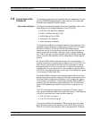
nals are then sent to the A21A1 YIG/Bias Controller PCB. This PCB
converts the analog signals to YIG main tuning coil current.
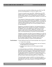
The main tuning coil current from A21A1 YIG/Bias Controller PCB
coarsely tunes the YIG-tuned Oscillator to within a few megahertz of
the final output frequency. The YIG phase-lock loop then fine tunes
the YIG-tuned oscillator to the exact output frequency via the FM (fine
tuning) coil.
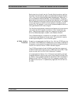
The fundamental frequency source signal is leveled by a PIN Diode at
-
tenuator that is part of the Switched Filter Assembly. This attenuator
is controlled by the Automatic Leveling Control (ALC) circuits that are
located on the A21A2 Source Control PCB. The input to the ALC cir
-
cuits is the DC feed-back signal from the leveling detectors located in
the Test Set Module.
Depending on the frequency of operation, the fundamental signal is
passed through one of four low-pass filters located in the Switched Fil
-
ter Assembly. The cut-off frequencies for these filters are 3.3 GHz,
5.5 GHz, 8.4 GHz, and 13.5 GHz, respectively. The signal is then
passed through a 20 GHz high pass filter before being routed either di-
rectly to the Test Set Module, or to the Down-Converter Assembly .
The signal is switched to the Down-Converter Assembly only when the
373XXA is operating in the low end portion of its frequency range. The
frequency of the output signal from the Down-Converter Assembly is
22.5 MHz to 2 GHz for Models 37311Aand 37317A and 40 MHz to 2
GHz for Models 37225B and above. The output signal from the
Down-Converter Assembly is routed to the Test Set Module.
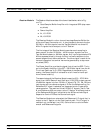
Test Set Module The Test Set Module consists of the items listed below; refer to Figure 7-2.
q
Transfer Switch assembly
q
Two Couplers (Models 37325A and above) or two Low Frequency
Bridges (Models 37317A and below)
q
Switched Doubler Module for 20-40 GHz operation (Model
37369A)
In the Test Set Module, the 22.5 MHz – 20 GHz signal from the signal
source module is switched (via the Transfer Switch) between the front
panel Port 1 and Port 2 connectors. The Transfer Switch is controlled
by the A9 Main Processor PCB to set the direction of signal flow for
the desired test (Port 1 = Forward; Port 2 = reverse). For operation be
-
tween 20 GHz and 40 GHz, the stimulus signal is routed to the
Switched Doubler Module before being sent to the Transfer Switch.
The stimulus signal is output to the DUT via directional couplers
mounted directly to the Port 1 and Port 2 front panel connectors. Note
that bridges are used instead of couplers in RF Models 37211B and
37217B.
ANALOG SUBSYSTEM ASSEMBLIES SYSTEM DESCRIPTION
7-8 373XXA MM


