


Table of Contents
7-1 INTRODUCTION ·························7-3
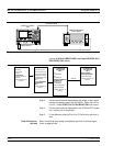
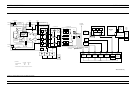
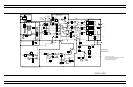
7-2 SYSTEM OVERVIEW ·······················7-3
7-3 ANALOG SUBSYSTEM ASSEMBLIES ·············7-7
Signal Source Module ·······················7-7
Test Set Module ··························7-8
A7 PCB, 10 MHz Timebase···················7-9
Receiver Module ·························7-10
A8, Source Lock/ Signal Separation and Control PCB ·····7-11
IF Section ·····························7-11
A7PCB,LO3 ··························7-12
A5 A/D Converter PCB ······················7-12
7-4 DIGITAL SUBSYSTEM ASSEMBLIES ·············7-13
A9 Main Processor PCB Assembly················7-13
A13 I/O Interface #1 PCB Assembly···············7-15
A14 I/O Interface #2 PCB Assembly···············7-15
A15 Graphics Processor PCB Assembly ·············7-16
A16 Hard Disk PCB Assembly··················7-16
Floppy Disk Drive Assembly ···················7-16
A24 VME Bus Terminator PCB ·················7-16
7-5 MAIN CHASSIS ASSEMBLIES ·················7-16
A17 System Motherboard Assembly···············7-16
Front Panel Assembly ······················7-16
Rear Panel Assembly·······················7-17
A18 Rear Panel Interface PCB··················7-17
Power Supply Module ······················7-18
Internal VGA Monitor ······················7-19
Chapter 7
System Description