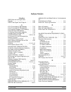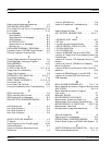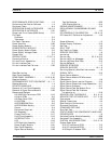
Subject Index
Number
37397A Source Lock Signal Path
Diagram ····················5-26
37397A Test Signal Path Diagram ······5-25
A
A13 I/O Interface #1 PCB Assembly ·····7-15
A14 I/O Interface #2 PCB Assembly ·····7-15
A15 Graphics Processor PCB Assembly · · · 7-16
A16 Hard Disk PCB Assembly ········7-16
A17 System Motherboard Assembly ·····7-16
A18 Rear Panel Interface PCB ········7-17
A18 REAR PANEL PCB ········8-22 -8 -24
A1-A9 and A13-A16 PCB Assemblies
Removal Diagram ················8-7
A1–A9 AND A13–A16 PCBS ··········8-6
A21A1 Source YIG Bias Control PCB·····8-32
A21A2 ADJUSTMENT
(37397A) ·················6-14 -6 -16
A21A2 Source Control PCB ··········8-31
A24 VME BUS TERMINATOR PCB ·····8-12
A31 Buffer Amplifier/Sampler Assembly · · · 8-28
A41 Power Amplifier Assembly ········8-27
A5 A/D Converter PCB ············7-12
A7 PCB, 10 MHz Timebase ···········7-9
A7 PCB, LO3 ··················7-12
A8 ADJUSTMENT (37397A) ·········6-13
A8, Source Lock/ Signal Separation and
Control PCB ··················7-11
A9 Main Processor PCB Assembly ······7-13
A9 PCB BBRAM CHIP ··········8-6-8-9
A9 PCB SRAM BATTERY ·······8-10 -8 -11
Acrobat Reader ·················1-3
Adjustments
A21A2 (37397A)···············6-14
A8 (37397A) ·················6-13
Frequency Calibration ············6-5
Internal Hardware Adjustments and
Calibratioin··················1-5
Introduction to ················6-3
LO1 Calibration ···············6-3
LO2 Calibration ···············6-4
RF Power/ALC Calibration ·········6-8
Source Lock Threshold ···········6-11
Adobe Acrobat ··················1-3
ANALOG SUBSYSTEM ASSEMBLIES 7-7 -7 -12
ANRITSU Service Centers ·········1-9,2-4
ASSOCIATED INFORMATION IN THIS MANUAL
5-3
Avoid Mechanical Shock ············C-4
Avoid Over Torquing Connectors ·······C-4
B
Boot-up Problems ················5-7
Boot-up Process Sequence ···········5-7
Buffer Amplifier/ Sampler(A31)········8-27
C
CALIBRATION AND MEASUREMENT CONDI
-
TIONS ······················4-3
CDROM·····················1-3
CHECKING THE SERVICE LOG·······3-4
Connector Maintenance
Cleaning ···················C-4
INTRODUCTION ··············C-3
Mechanical Shock ··············C-4
Pin Depth Problems ·············C-3
Pin Depth Tolerances ············C-4
Precautions··················C-3
Repair/Maintenance ·············C-5
Teflon Tuning Washer ············C-4
Torque ····················C-4
Visual Inspection···············C-5
Consummsable Parts ··············2-6
COVERS ··················8-4-8-5
CRT Display Test Failures: ··········5-21
D
Diagnostic Menus
INTRODUCTION ··············A-3
Diagnostics Menus
H/W (Hardware) Calibrations ········A-5
Installed Options···············A-4
Peripheral Tests ···············A-4
Read Service Log···············A-3
Start Self Test ················A-3
Troubleshooting ···············A-4
DIAGNOSTICS MENUS ·········A-3-A-6
Diagnostics Menus Flowchart ·········A-7
DIGITAL SUBSYSTEM ASSEMBLIES 7-13 -7 -15
DigitalSubsystem Block Diagram·······7-14
DISK RELATED ERROR MESSAGES ····B-3
Down Converter Assembly ··········8-33
372XXB MM Index-3


