


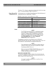
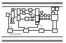

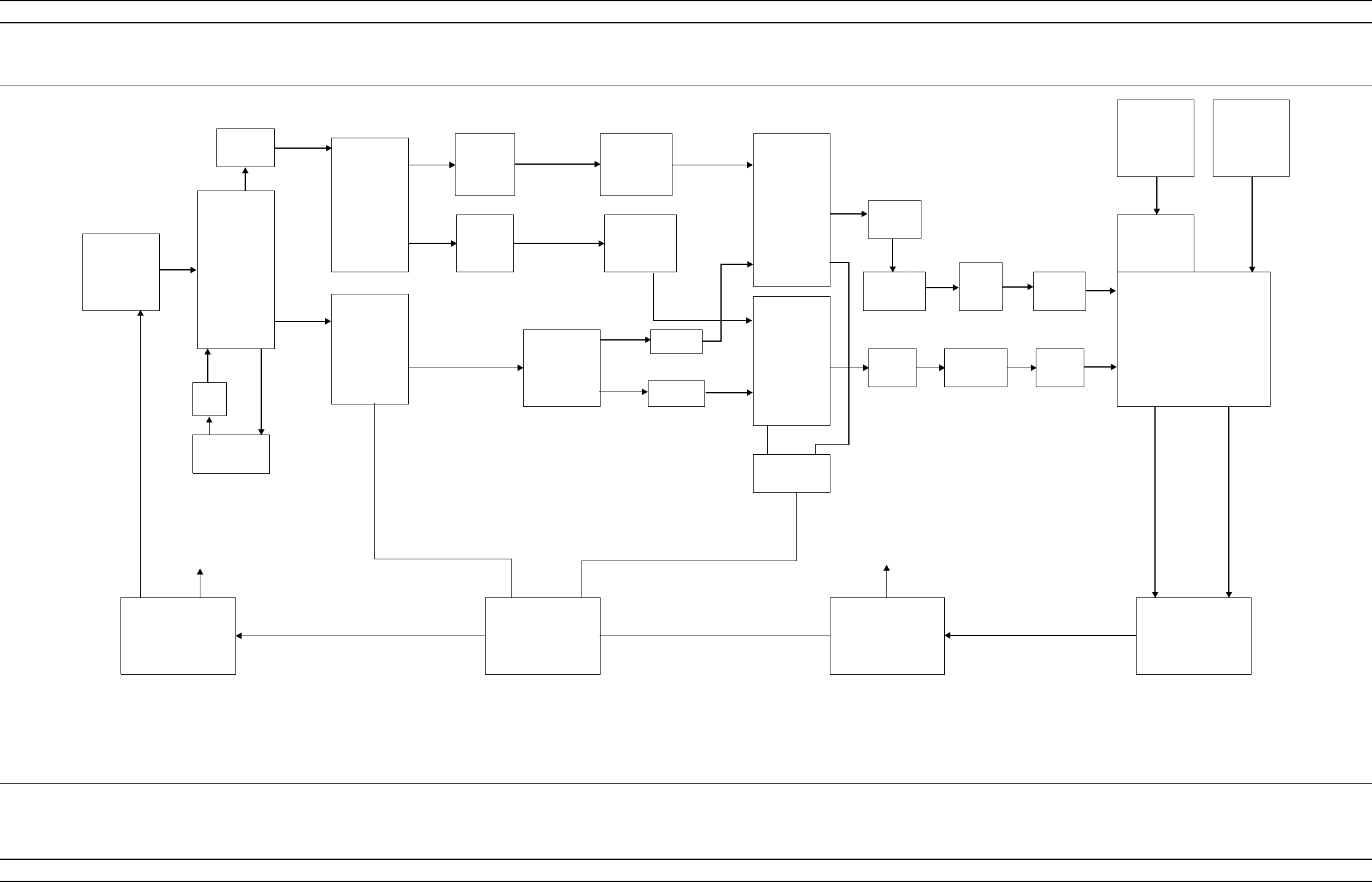
5-26 373XXA MM
SIGNAL PATHS TROUBLESHOOTING
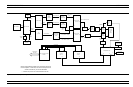
YIG Oscillator
X4
(SQM)
Reverse
Switched Filter
Down
Converter
A21A2 PCB
Sampler/BufferAmp
X2
(SDM)
3dBpad
X4
(SQM)
Forward
MUX Coupler
(reverse)
3dBPad
Transfer Switch
(RefA/ Ref B
Control)
37 GHz
HiPass Filter
37 GHz
HiPass Filter
Shaped Pad
Shaped Pad
MUX Coupler
(forward)
A21A1 PCB
A4 PCB
Reference IF Processor
SPDT Switch
J4
J5
RefA
Ref B 38-65 GHz
RefA 38-65 GHz
Ref B
A8 PCB
Source Lock/ RF
Component Control
PowerAmp
Second LO
(A2 PCB)
(25-272MHz)
First LO
(A1 PCB)
(357-536MHz)
RefA 40MHz - 38GHz
Ref B 40MHz - 38GHz
Rear
Panel
Access
Loop **
40MHz-65GHz (RefA)
40MHz -
65GHz (Ref B)
ALC Control PCB
49808-3
Ref A
J7
J8
Ref B
2.5 MHz CW
2.5 MHz CW
J4
J2J1
J1
J3
RefA 38-65 GHz
Ref B
DC
voltage
38-65
GHz
DC voltage (6 MHz / Volt)
J4
J1
J4J4
J5
J5
DCV
DCV
J1
J3
J2
YIG tuning currents
Digital andAnalog Control
40MHz-
2GHz
6.3-
8.3GHz
2-20GHz
40MHz-
19GHz
9.5-
16.25GHz
40MHz-38GHz
SDM Control
Bias Voltages to YIG,
Switched Filter
Down Converter, SAM
Control of SPDT
switch, transfer switch,
buffer amp, power
amp,ALC control
J5
J5 J3
J1
3dBpad
3dBpad
16.8 GHz
Lowpass
Filter
15 dB
Pad
NOTE: Sampler/Buffer amplifiers are individually matched to
Power Amplifiers. If either fails, both should be replaced with
another matched set, part number ND53249.
3dBPad
** Indicates not
p
resent on model 37297B or 37277B
3dBpad
Figure 5-4. 37397A Source Lock Signal Path Diagram