


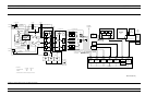
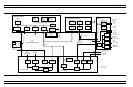

Each output circuit path from the Transfer Switch contains a splitter.
One path from each splitter goes to the associated directional coupler
(Port 1/Port 2) and the other path feeds the associated “Reference” in
-
put of the Receiver Module (RA/RB), via a level detector. The output
generated by the two parallel configured level detectors is a DC signal
that corresponds to the output level of the stimulus signal. This signal
is the input signal for the ALC circuits located in the signal source
module. Only the detector in the currently selected sweep direction ac
-
tually generates the ALC control signal.
The Test Set simultaneously receives the reflected and transmitted de
-
vice-under-test (DUT) signals via the Port 1/Port 2 directional cou
-
plers. These two test signals, along with a sample of the output RF
stimulus (Reference) signal, are sent to the Receiver Module.
The a1 Reference signal is routed out of, and back into, the 373XXA
via extension loop located on the rear panel. This allows for injection
of user supplied signals in lieu of internal signals.
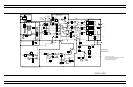
A7 PCB, 10 MHz
Timebase
Except for units equipped with Option 10 or 10A, the A7 PCB contains
the 10 MHz TCXO Reference Timebase that is the master timebase for
the system. It also contains the signal distribution and switching func-
tions for all External/Internal 10 MHz reference signals.
The A7 PCB provides the fixed 2.42 MHz Local Oscillator signal and
the 80 kHz Calibration signal to the IF PCBS (A3, A4, and A6). These
signals are derived from the 10 MHz Reference Timebase.
Units equipped with Option 10 or 10A have a high-stability ovenized
timebase mounted inside the rear panel directly above the Power Sup
-
ply Module. This timebase replaces the standard 10 MHz timebase lo
-
cated on the A7 PCB. The output from this timebase is routed to the
A7 PCB for distribution. It is powered by regulated +24 vdc from the
A7 PCB.
SYSTEM DESCRIPTION ANALOG SUBSYSTEM ASSEMBLIES
373XXA MM 7-9