Appendix C Functional Description C-9
C.1.6 Memory System
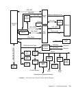
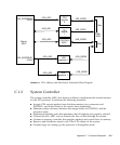
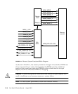
The memory system (FIGURE C-3) consists of three components: the system controller
(Marvin ASIC), the buffered crossbar chip (K9+ ASIC), and the memory module. The
Marvin ASIC generates memory addresses and control signals to the memory
module. The Marvin ASIC also coordinates the data transfers among the DIMMs
through two 144-bit-wide processor data buses (UPA_DATA0 and UPA_DATA1) and
the two I/O data bus; UPA_DATA2 and UPA_DATA3.
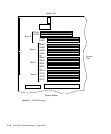
DIMMs are organized in banks in groups of four (quads). DIMM capacities of
16-Mbyte, 32-Mbyte, 64-Mbyte, and 128-Mbyte are supported by the memory
module. When all DIMM banks are populated with 128-Mbyte DIMMs, maximum
memory capacity is 2 gigabytes.
Organizing the four DIMM banks with 128-Mbyte (plus ECC bit) DIMMs allows
data streams to be transferred on a 512-bit-wide (plus ECC) memory data bus.
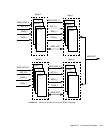
UPA_DATA0, UPA_DATA1, UPA_DATA2, and UPA_DATA3 bus switching The
XB9+ ASIC is controlled by the Marvin ASIC and performs all data bus switching.


