C-10 Sun Ultra 60 Service Manual • August 2001
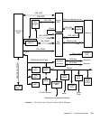
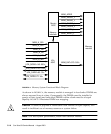
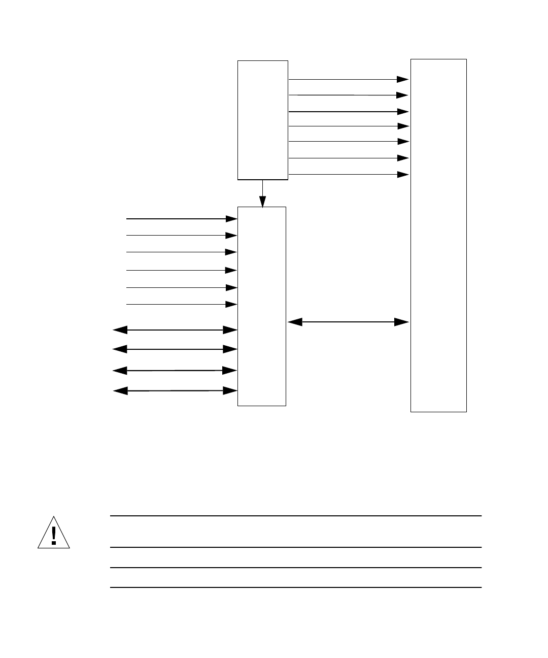
FIGURE C-3 Memory System Functional Block Diagram
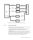
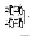
As shown in FIGURE C-4, the memory module is arranged in four banks. DIMMs are
always accessed four at a time. Consequently, the DIMMs must be installed in
groups of four (quad) and individual DIMMs within a bank must be of equal
capacity.
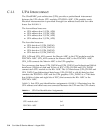
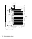
FIGURE C-5 illustrates DIMM row mapping.
Caution – Failure to populate a DIMM bank with DIMMs of equal capacity will
result in inefficient use of memory resource or system failure.
Note – For best system performance, install four identical DIMMs.
Memory
module
UPA_DATA1<143..000>
UPA_DATA2<63..00>
Marvin
MEM_ADDR
MEM_RASA0_L
MEM_CASR2_L
MEM_A_WR
MEM_B_WR
K9+
ASIC
Memory
interface
MEM_DAT<575..000>
ASIC
MEM_RASA2_L
MEM_CASR0_L
MEM_A_RD
MEM_B_RD
MEM_A_SEL
MEM_B_SEL
MEM_WRR2_L
MEM_WRR0_L
UPA_DATA0<143..000>
UPA_DATA3<71..00>


