AMD Geode™ SC1200/SC1201 Processor Data Book 129
SuperI/O Module
32579B
5.8 Legacy Functional Blocks
This section briefly describes the following blocks that pro-
vide legacy device functions:
• Parallel Port. (Similar to Parallel Port in the National
Semiconductor PC87338.)
• Serial Port 1 and Serial Port 2 (SP1 and SP2), UART
functionality for both SP1 and SP2. (Similar to SCC1 in
the National Semiconductor PC87338.)
• Infrared Communications Port / Serial Port 3 function-
ality. (Similar to SCC2 in the National Semiconductor
PC87338.)
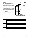
The description of each Legacy block includes a general
description, register maps, and bit maps.
5.8.1 Parallel Port
The Parallel Port supports all IEEE1284 standard commu-
nication modes: Compatibility (known also as Standard or
SPP), Bidirectional (known also as PS/2), FIFO, EPP
(known also as Mode 4) and ECP (with an optional
Extended ECP mode).
5.8.1.1 Parallel Port Register and Bit Maps
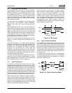
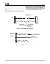
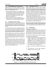
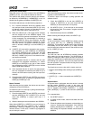
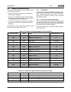
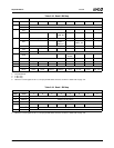
The Parallel Port register maps (Table 5-33 and Table 5-34)
are grouped according to first and second level offsets.
EPP and second level offset registers are available only
when the base address is 8-byte aligned.
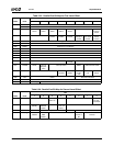
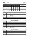
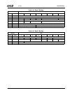
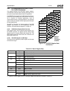
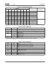
Parallel Port functional block bit maps are shown in Table 5-
35 and Table 5-36.
Table 5-33. Parallel Port Register Map for First Level Offset
First Level Offset Type Name Modes (ECR Bits) 7 6 5
000h R/W DATAR. PP Data 000 or 001
000h W AFIFO. ECP Address FIFO 011
001h RO DSR. Status All Modes
002h R/W DCR. Control All Modes
003h R/W ADDR. EPP Address 100
004h R/W DATA0. EPP Data Port 0 100
005h R/W DATA1. EPP Data Port 1 100
006h R/W DATA2. EPP Data Port 2 100
007h R/W DATA3. EPP Data Port 3 100
400h W CFIFO. PP Data FIFO 010
400h R/W DFIFO. ECP Data FIFO 011
400h R/W TFIFO. Test FIFO 110
400h RO CNFGA. Configuration A 111
401h RO CNFGB. Configuration B 111
402h R/W ECR. Extended Control All Modes
403h R/W EIR. Extended Index All Modes
404h R/W EDR. Extended Data All Modes
405h R/W EAR. Extended Auxiliary Status All Modes
Table 5-34. Parallel Port Register Map for Second Level Offset
Second Level Offset Type Name
00h R/W Control0. Control Register 0
02h R/W Control2. Control Register 2
04h R/W Control4. Control Register 4
05h R/W PP Confg0. Parallel Port Configuration Register 0


