AMD Geode™ SC1200/SC1201 Processor Data Book 81
General Configuration Block
32579B
4.4 High-Resolution Timer
The SC1200/SC1201 processor provides an accurate time
value that can be used as a time stamp by system soft-
ware. This time is called the High-Resolution Timer. The
length of the timer value can be extended via software. It is
normally enabled while the system is in the C0 and C1
states. Optionally, software can be programmed to enable
use of the High-Resolution Timer during C3 state and/or
S1 state as well. In all other power states the High-Resolu-
tion Timer is disabled.
4.4.1 Functional Description
The High-Resolution Timer is a 32-bit free-running count-
up timer that uses the oscillator clock or the oscillator clock
divided by 27. Bit TMCLKSEL of the TMCNFG register
(Offset 0Dh[1]) can be set via software to determine which
clock should be used for the High-Resolution Timer.
When the most significant bit (bit 31) of the timer changes
from 1 to 0, bit TMSTS of the TMSTS register (Offset
0Ch[0]) is set to 1. When both bit TMSTS and bit TMEN
(Offset 0Dh[0]) are 1, an interrupt is asserted. Otherwise,
the interrupt is de-asserted. This interrupt enables software
emulation of a larger timer.
The High-Resolution Timer interrupt is routed to an IRQ
signal. The IRQ signal is programmable via the INTSEL
register (Offset 38h). For more information about this regis-
ter, see section Section 4.2 "Pin Multiplexing, Interrupt
Selection, and Base Address Registers" on page 72.
System software uses the read-only TMVALUE register
(Offset 08h[31:0]) to read the current value of the timer.
The TMVALUE register has no default value.
The input clock (derived from the 27 MHz crystal oscillator)
is enabled when:
• The GX1 module’s internal SUSPA# signal is 1.
or
• The GX1 module’s internal SUSPA# signal is 0 and bit
TM27MPD (Offset 0Dh[2]) is 0.
The input clock is disabled, when the GX1 module’s inter-
nal SUSPA# signal is 0 and the TM27MPD bit is 1.
For more information about signal SUSPA# see Section
4.4.2.1 "Usage Hints" on page 81 and the AMD Geode™
GX1 Processor Data Book.
The High-Resolution Timer function resides on the internal
Fast-PCI bus and its registers are in General Configuration
Block address space. Only one complete register should
be accessed at-a-time (e.g., DWORD access should be
used for DWORD wide registers and byte access should be
used for byte-wide registers).
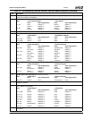
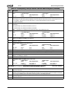
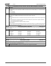
4.4.2 High-Resolution Timer Registers
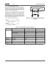
Table 4-4 on page 82 describes the registers for the High-
Resolution Timer (TIMER).
4.4.2.1 Usage Hints
• SMM code should set bit 2 of the TMCNFG register to 1
when entering ACPI C3 state if the High-Resolution
Timer should be disabled. If this is not done, the High-
Resolution Timer is functional during C3 state.
• SMM code should set bit 2 of the TMCNFG register to 1
when entering ACPI S1 state if the High-Resolution
Timer should be disabled. If this is not done, the High-
Resolution Timer is functional during S1 state.
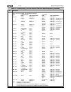
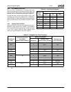
Offset 04h WATCHDOG Status Register - WDSTS (R/WC) Reset Value: 00h
This register contains WATCHDOG status information.
7:4 Reserved. Write as read.
3 WDRST (WATCHDOG Reset Asserted). (Read Only) This bit is set to 1 when WATCHDOG Reset is asserted. It is set to
0 when POR# is asserted, or when the WDOVF bit is set to 0.
2 WDSMI (WATCHDOG SMI Asserted). (Read Only) This bit is set to 1 when WATCHDOG SMI is asserted. It is set to 0
when POR# is asserted, or when the WDOVF bit is set to 0.
1 WDINT (WATCHDOG Interrupt Asserted). (Read Only) This bit is set to 1 when the WATCHDOG Interrupt is asserted. It
is set to 0 when POR# is asserted, or when the WDOVF bit is set to 0.
0 WDOVF (WATCHDOG Overflow). This bit is set to 1 when the WATCHDOG Timer reaches 0. It is set to 0 when POR# is
asserted, or when a 1 is written to this bit by software. Other system reset sources do not affect this bit.
Offset 05h-07h Reserved - RSVD
Table 4-3. WATCHDOG Registers (Continued)
Bit Description


