250 AMD Geode™ SC1200/SC1201 Processor Data Book
Core Logic Module - SMI Status and ACPI Registers - Function 1
32579B
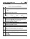
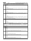
13 SLP_EN (Sleep Enable). (Write Only) Allow the system to sequence into the sleeping state associated with the SLP_TYPx
(bits [12:10]).
0: Disable.
1: Enable.
This is a write only bit and reads of this bit always return a 0.
The ACPI state machine always waits for an SMI (any SMI) to be generated and serviced before transitioning into a Sleep
state.
If F1BAR1+I/O Offset 18h[9] = 1, an SMI is generated when SLP_EN is set.
Top level SMI status is reported at F1BAR0+I/O Offset 00h/02h[2].
Second level SMI status is reported at F1BAR0+I/O Offset 20h/22h[2].
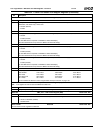
12:10 SLP_TYPx (Sleep Type). Defines the type of Sleep state the system enters when SLP_EN (bit 13) is set.
000: Sleep State S0 (Full on) 100: Sleep State SL4
001: Sleep State SL1 101: Sleep State SL5 (Soft off)
010: Sleep State SL2 110: Reserved
011: Sleep State SL3 111: Reserved
9:3 Reserved. Set to 0.
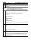
2 GBL_RLS (Global Release). (Write Only) This write only bit is used by ACPI software to raise an event to the BIOS soft-
ware (i.e., it generates an SMI to pass execution control to the BIOS).
0: Disable.
1: Enable.
This is a write only bit and reads of this bit always return a 0.
To generate an SMI, ACPI software writes the GBL_RLS bit which in turn sets the BIOS_STS bit (F1BAR1+I/O Offset
0Eh[0]) and raises a PME. For the PME to generate an SMI, set BIOS_EN (F1BAR1+I/O Offset 0Fh[0] to 1).
The top level SMI status is reported at F1BAR0+I/O offset 00h/02h.
Second level status is at F1BAR0+I/O Offset 22h[5].
1 BM_RLD (Bus Master RLD). If the processor is in the C3 state and a bus master request is generated, force the processor
to transition to the C0 state.
0: Disable.
1: Enable
0 SCI_EN (System Control Interrupt Enable). Globally selects power management events (PMEs) reported in PM1A_STS
and GPE0_STS (F1BAR1+I/O Offset 08h and 10h) to be either an SCI or SMI type of interrupt.
0: APM Mode, generates an SMI and status is reported at F1BAR0+I/O Offset 00h/02h[0].
1: ACPI Mode, generates an SCI if the corresponding PME enable bit is set and status is reported at F1BAR1+I/O Offset
08h and 10h.
Note: This bit enables the ACPI state machine.
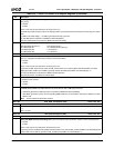
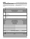
Offset 0Eh ACPI_BIOS_STS Register (R/W) Reset Value: 00h
7:1 Reserved. Must be set to 0.
0 BIOS_STS (BIOS Status Release). When 1 is written to the GLB_RLS bit (F1BAR1+I/O Offset 0Ch[2]), this bit is also set
to 1.
Write 1 to clear.
Offset 0Fh ACPI_BIOS_EN Register (R/W) Reset Value: 00h
7:2 Reserved. Must be set to 0.
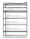
1 BIOS_RLS (BIOS Release). (Write Only) When this bit is asserted, allow the BIOS to release control of the global lock.
0: Disable.
1: Enable.
This is a write only bit and reads of this bit always return a 0.
To generate an SCI, the BIOS writes the BIOS_RLS bit which in turn sets the GBL_STS bit (F1BAR1+I/O Offset 08h[5]) and
raises a PME. For the PME to generate an SCI, set GBL_EN (F1BAR1+I/O Offset 0Ah[5] to 1).
Table 6-34. F1BAR1+I/O Offset: ACPI Support Registers (Continued)
Bit Description


