


AMD Geode™ SC1200/SC1201 Processor Data Book 77
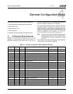
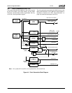
General Configuration Block
32579B
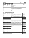
19:18 PLL1 and TV Encoder Clock Frequency. PLL1 supplies the clock for the TV Encoder.
00: TV Encoder clock is 27 MHz from crystal oscillator. PLL1 is powered down.
01: TV Encoder clock is PLL1 output. PLL1 output is 27 MHz.
10: TV Encoder clock is PLL1 output. PLL1 output is 24.545454 MHz.
11: TV Encoder clock is PLL1 output. PLL1 output is 29.5 MHz.
17 HSYNC Timing. HSYNC timing control for TFT.
0: HSYNC timing suited for CRT.
1: HSYNC timing suited for TFT.
16 Delay HSYNC. HSYNC delay by two TFT clock cycles.
0: There is no delay on HSYNC.
1: HYSNC is delayed twice by rising edge of TFT clock. Enables delay between VSYNC and HSYNC suited for TFT dis-
play.
15 Reserved. Write as read.
14 IBUS16 (Invert BUS16). This bit inverts the meaning of MCR[3] (bit 3 of this register).
0: BUS16 is as described for MCR[3].
1: BUS16 meaning is inverted: if MCR[3] = 0, ROMCS# access is 16 bits wide; if MCR[3] = 1, ROMCS# access is 8 bits
wide.
13 Reserved. Must be set to 0.
12 IO1ZWS (Enable ZWS# for IOCS1# Access). This bit enables internal activation of ZWS# (Zero Wait States) control for
IOCS1# access.
0: ZWS# is not active for IOCS1# access.
1: ZWS# is active for IOCS1# access.
11 IO0ZWS (Enable ZWS# for IOCS0# Access). This bit enables internal activation of ZWS# (Zero Wait States) control for
IOCS0# access.
0: ZWS# is not active for IOCS0# access.
1: ZWS# is active for IOCS0# access.
10 DOCZWS (Enable ZWS# for DOCCS# Access). This bit enables internal activation of ZWS# (Zero Wait States) control for
DOCCS# access.
0: ZWS# is not active for DOCCS# access.
1: ZWS# is active for DOCCS# access.
9 ROMZWS (Enable ZWS# for ROMCS# Access). This bit enables internal activation of ZWS# (Zero Wait States) control for
ROMCS# access.
0: ZWS# is not active for ROMCS# access.
1: ZWS# is active for ROMCS# access.
8 IO1_16 (Enable 16-Bit Wide IOCS1# Access). This bit enables the16-line access to IOCS1# in the Sub-ISA interface.
0: 8-bit wide IOCS1# access is used.
1: 16-bit wide IOCS1# access is used.
7 IO0_16 (Enable 16-Bit Wide IOCS0# Access). This bit enables the 16-line access to IOCS0# in the Sub-ISA interface.
0: 8-bit wide IOCS0# access is used.
1: 16-bit wide IOCS0# access is used.
6 DOC16 (Enable 16-Bit Wide DOCCS# Access). This bit enables the 16-line access to DOCCS# in the Sub-ISA interface.
0: 8-bit wide DOCCS# access is used.
1: 16-bit wide DOCCS# access is used.
5 Reserved. Write as read.
4 IRTXEN (Infrared Transmitter Enable). This bit enables drive of Infrared transmitter output.
0: IRTX+SOUT3 line (ball C11) is HiZ.
1: IRTX+SOUT3 line (ball C11) is enabled.
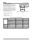
Table 4-2. Pin Multiplexing, Interrupt Selection, and Base Address Registers (Continued)
Bit Description