202 AMD Geode™ SC1200/SC1201 Processor Data Book
Core Logic Module - Bridge, GPIO, and LPC Registers - Function 0
32579B
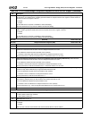
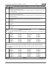
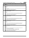
25 Writes Result in Chip Select. When this bit is set to 1, writes to configured memory address (base address configured in
F0 Index 78h; range configured in bits [18:0]) cause DOCCS# to be asserted.
0: Disable.
1: Enable.
24 Reads Result in Chip Select. When this bit is set to 1, reads from configured memory address (base address configured in
F0 Index 78h; range configured in bits [18:0]) cause DOCCS# to be asserted.
0: Disable.
1: Enable.
23:19 Reserved. Must be set to 0.
18:0 DOCCS# Memory Address Range. This 19-bit mask is used to qualify accesses on which DOCCS# is asserted by mask-
ing the upper 19 bits of the incoming PCI address (AD[31:13]).
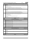
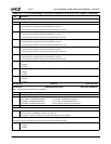
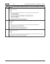
Index 80h Power Management Enable Register 1 (R/W) Reset Value: 00h
7:6 Reserved. Must be set to 0.
5 Codec SDATA_IN SMI. When set to 1, this bit allows an SMI to be generated in response to an AC97 codec producing a
positive edge on SDATA_IN.
0: Disable.
1: Enable.
Top level SMI status is reported at F1BAR0+I/O Offset 00h/02h[0].
Second level SMI status is reported at F0 Index 87h/F7h[2].
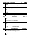
4 Video Speedup. Any video activity, as decoded from the serial connection (PSERIAL) from the GX1 module disables clock
throttling (via internal SUSP#/SUSPA# handshake) for a configurable duration when system is power-managed using CPU
Suspend modulation.
0: Disable.
1: Enable.
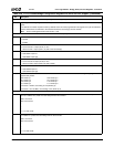
The duration of the speedup is configured in the Video Speedup Timer Count Register (F0 Index 8Dh). Detection of an
external VGA access (3Bx, 3Cx, 3Dx and A000h-B7FFh) on the PCI bus is also supported. This configuration is non-stan-
dard, but it does allow the power management routines to support an external VGA chip.
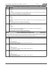
3 IRQ Speedup. Any unmasked IRQ (per I/O Ports 021h/0A1h) or SMI disables clock throttling (via internal SUSP#/SUSPA#
handshake) for a configurable duration when system is power-managed using CPU Suspend modulation.
0: Disable.
1: Enable.
The duration of the speedup is configured in the IRQ Speedup Timer Count Register (F0 Index 8Ch).
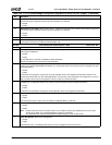
2 Traps. Globally enable all power management I/O traps.
0: Disable.
1: Enable.
This excludes the audio I/O traps, which are enabled via F3BAR0+Memory Offset 18h.
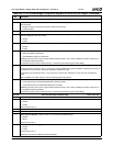
1 Timers. General Purpose and Device Idle Timers.
0: Disable.
1: Enable.
Note: Disable at this level does not reload the timers on the enable. The timers are disabled at their current counts.
This bit has no affect on the Suspend Modulation register (F0 Index 94h).
Only applicable when in APM mode (F1BAR1+I/O Offset 0Ch[0] = 0) and not ACPI mode.
0 Power Management. Global power management.
0: Disable.
1: Enable.
This bit must be set to 1 immediately after POST for power management resources to function.
Table 6-29. F0: PCI Header/Bridge Configuration Registers for GPIO and LPC Support (Continued)
Bit Description


