146 AMD Geode™ SC1200/SC1201 Processor Data Book
Core Logic Module
32579B
6.2.3.4 UltraDMA/33 Mode
The IDE controller of the Core Logic module supports
UltraDMA/33. It utilizes the standard IDE Bus Master func-
tionality to interface, initiate and control the transfer.
UltraDMA/33 definition also incorporates a Cyclic Redun-
dancy Checking (CRC) error checking protocol to detect
errors.
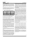
The UltraDMA/33 protocol requires no extra signal pins on
the IDE connector. The IDE controller redefines three stan-
dard IDE control signals when in UltraDMA/33 mode.
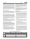
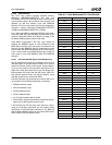
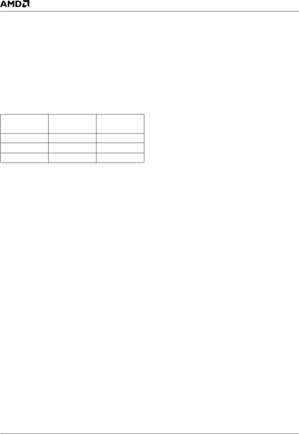
These definitions are shown in Table 6-2.
All other signals on the IDE connector retain their func-
tional definitions during the UltraDMA/33 operation.
IDE_IOW# is defined as STOP for both read and write
transfers to request to stop a transaction.
IDE_IOR# is redefined as DMARDY# for transferring data
from the IDE device to the IDE controller. It is used by the
IDE controller to signal when it is ready to transfer data and
to add wait states to the current transaction. IDE_IOR# sig-
nal is defined as STROBE for transferring data from the
IDE controller to the IDE device. It is the data strobe signal
driven by the IDE controller on which data is transferred
during each rising and falling edge transition.
IDE_IORDY is redefined as STROBE for transferring data
from the IDE device to the IDE controller during a read
cycle. It is the data strobe signal driven by the IDE device
on which data is transferred during each rising and falling
edge transition. IDE_IORDY is defined as DMARDY# dur-
ing a write cycle for transferring data from the IDE control-
ler to the IDE device. It is used by the IDE device to signal
when it is ready to transfer data and to add wait states to
the current transaction.
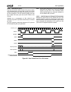
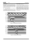
UltraDMA/33 data transfer consists of three phases, a star-
tup phase, a data transfer phase and a burst termination
phase.
The IDE device begins the startup phase by asserting
IDE_DREQ. When ready to begin the transfer, the IDE con-
troller asserts IDE_DACK#. When IDE_DACK# is asserted,
the IDE controller drives IDE_CS0# and IDE_CS1#
asserted, and IDE_ADDR[2:0] low. For write cycles, the
IDE controller negates STOP, waits for the IDE device to
assert DMARDY#, and then drives the first data WORD
and STROBE signal. For read cycles, the IDE controller
negates STOP, and asserts DMARDY#. The IDE device
then sends the first data WORD and asserts STROBE.
The data transfer phase continues the burst transfers with
the Core Logic and the IDE via providing data, toggling
STROBE and DMARDY#. The IDE_DATA[15:0] is latched
by receiver on each rising and falling edge of STROBE.
The transmitter can pause the burst cycle by holding
STROBE high or low, and resume the burst cycle by again
toggling STROBE. The receiver can pause the burst cycle
by negating DMARDY# and resumes the burst cycle by
asserting DMARDY#.
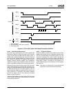
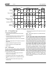
The current burst cycle can be terminated by either the
transmitter or the receiver. A burst cycle must first be
paused as described above before it can be terminated.
The IDE controller can then stop the burst cycle by assert-
ing STOP, with the IDE device acknowledging by negating
IDE_DREQ. The IDE device then stops the burst cycle by
negating IDE_DREQ and the IDE controller acknowledges
by asserting STOP. The transmitter then drives the
STROBE signal to a high level. The IDE controller then
puts the result of the CRC calculation onto the
IDE_DATA[15:0] while de-asserting IDE_DACK#. The IDE
device latches the CRC value on the rising edge of
IDE_DACK#.
The CRC value is used for error checking on UltraDMA/33
transfers. The CRC value is calculated for all data by both
the IDE controller and the IDE device during the UltraDMA/
33 burst transfer cycles. This result of the CRC calculation
is defined as all data transferred with a valid STROBE edge
while IDE_DACK# is asserted. At the end of the burst
transfer, the IDE controller drives the result of the CRC cal-
culation onto IDE_DATA[15:0] which is then strobed by the
de-assertion of IDE_DACK#. The IDE device compares the
CRC result of the IDE controller to its own and reports an
error if there is a mismatch.
The timings for UltraDMA/33 are programmed into the
DMA control registers:
• Channel 0 Drive 0 DMA Control Register (F2 Index 44h)
• Channel 0 Drive 1 DMA Control Register (F2 Index 4Ch)
• Channel 1 Drive 0 DMA Control Register (F2 Index 54h)
• Channel 1 Drive 1 DMA Control Register (F2 Index 5Ch)
The bit formats for these registers are described in Table 6-
35 on page 256. Note that F2 Index 44h[20] is used to
select either Multiword or UltraDMA mode. Bit 20 = 0
selects Multiword DMA mode. If bit 20 = 1, then UltraDMA/
33 mode is selected. Once mode selection is made using
this bit, the remaining DMA Control registers also operate
in the selected mode.
Also listed in the bit formats are recommended values for
both Multiword DMA Modes 0-2 and UltraDMA/33 Modes
0-2. Note that these are only recommended settings and
are not 100% tested.
Table 6-2. UltraDMA/33 Signal Definitions
IDE Controller
Channel Signal
UltraDMA/33
Read Cycle
UltraDMA/33
Write Cycle
IDE_IOW# STOP STOP
IDE_IOR# DMARDY# STROBE
IDE_IORDY STROBE DMARDY#


