92 AMD Geode™ SC1200/SC1201 Processor Data Book
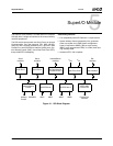
SuperI/O Module
32579B
5.3 Configuration Structure / Access
This section describes the structure of the configuration
register file, and the method of accessing the configuration
registers.
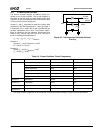
5.3.1 Index-Data Register Pair
The SIO configuration access is performed via an Index-
Data register pair, using only two system I/O byte locations.
The base address of this register pair is determined
according to the state of the IO_SIOCFG_IN bit field of the
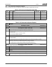
Core Logic module (F5BAR0+I/O Offset 00h[26:25]). Table
5-1 shows the selected base addresses as a function of the
IO_SIOCFG_IN bit field.
The Index Register is an 8-bit R/W register located at the
selected base address (Base+0). It is used as a pointer to
the configuration register file, and holds the index of the
configuration register that is currently accessible via the
Data Register. Reading the Index Register returns the last
value written to it (or the default of 00h after reset).
The Data Register is an 8-bit virtual register, used as a
data path to any configuration register. Accessing the data
register results with physically accessing the configuration
register that is currently pointed by the Index Register.
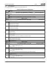
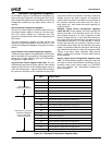
5.3.2 Banked Logical Device Registers
Each functional block is associated with a Logical Device
Number (LDN). The configuration registers are grouped
into banks, where each bank holds the standard configura-
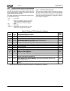
tion registers of the corresponding logical device. Table 5-2
shows the LDNs of the device functional blocks.
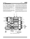
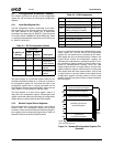
Figure 5-3 shows the structure of the standard PnP config-
uration register file. The SIO Control And Configuration
registers are not banked and are accessed by the Index-
Data register pair only (as described above). However, the
Logical Device Control and Configuration registers are
duplicated over eight banks for eight logical devices. There-
fore, accessing a specific register in a specific bank is per-
formed by two-dimensional indexing, where the LDN
register selects the bank (or logical device), and the Index
register selects the register within the bank. Accessing the
Data register while the Index register holds a value of 30h
or higher results in a physical access to the Logical Device
Configuration registers currently pointed to by the Index
register, within the logical device bank currently selected by
the LDN register.
Figure 5-3. Standard Configuration Register File
Structure
Table 5-1. SIO Configuration Options
IO_SIOCFG_IN
Settings
I/O Address
Description
Index
Register
Data
Register
00 - - SIO disabled
01 - - Configuration
access disabled
10 002Eh 002Fh Base address 1
selected
11 015Ch 015Dh Base address 2
selected
Table 5-2. LDN Assignments
LDN Functional Block Reference
00h Real-Time Clock (RTC) Page 98
01h System Wakeup Control (SWC) Page 100
02h Infrared Communication Port
(IRCP) or Serial Port 3 (SP3)
Page 101
03h Serial Port 1 (SP1) Page 102
05h ACCESS.bus 1 (ACB1) Page 103
06h ACCESS.bus 2 (ACB2)
07h Parallel Port (PP) Page 104
08h Serial Port 2 (SP2) Page 102
07h
20h
30h
60h
75h
FEh
Logical Device Number Register
SIO Configuration Registers
Logical Device Control Register
Standard Logical Device
Banks
(One per Logical Device)
2Fh
F0h
Bank
63h
74h
70h
71h
Standard Registers
Special (Vendor-defined)
Configuration Registers
Logical Device
Select


